


Other Parts Discussed in Thread: OMAPL138
Hi,
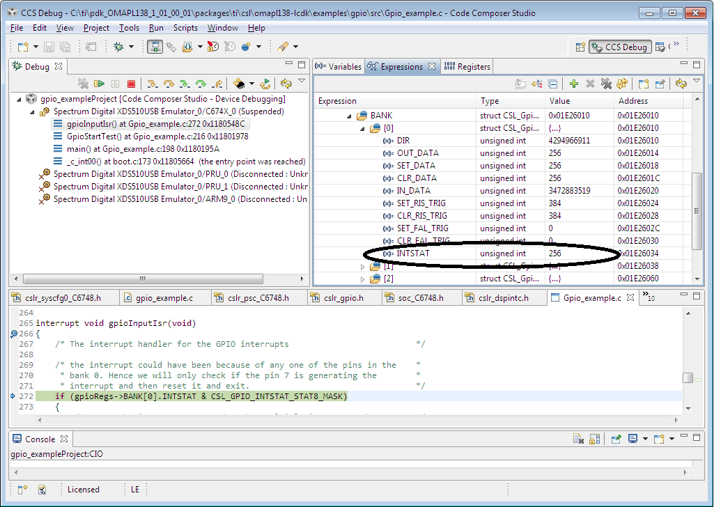
OMAP L138 DSP is receiving GPIO interrupts in the same bank (GPIO Bank 4) on different GPIO pins, at the same instant.On receiving GPIO bank 4 interrupt, I read INTSTAT45 register and found that only one of the GPIO pins has raised the interrupt.Is it that other interrupts have been missed?
I have searched for similar posts in forum but didnt find a solution.
Thanks
Sreejaya


