This thread has been locked.

If you have a related question, please click the "Ask a related question" button in the top right corner. The newly created question will be automatically linked to this question.

How to verify the cache locked data?

Other Parts Discussed in Thread: SYSBIOS, OMAP3530

Dear TI forum supporters:

I have tried to locked some data I moved via PLE in cache lines (ex. way 0) of cortex A8, but I have no idea how to use them.

I would first like to verify the correctness of data in the cache by following the article on forum like this:

http://e2e.ti.com/support/arm/sitara_arm/f/791/t/204656.aspx

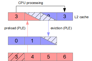
In the article, the author mentioned using a loop, events (L2 miss, and AXI), and read virtual address(ex. 0x80..)

to verify the data.


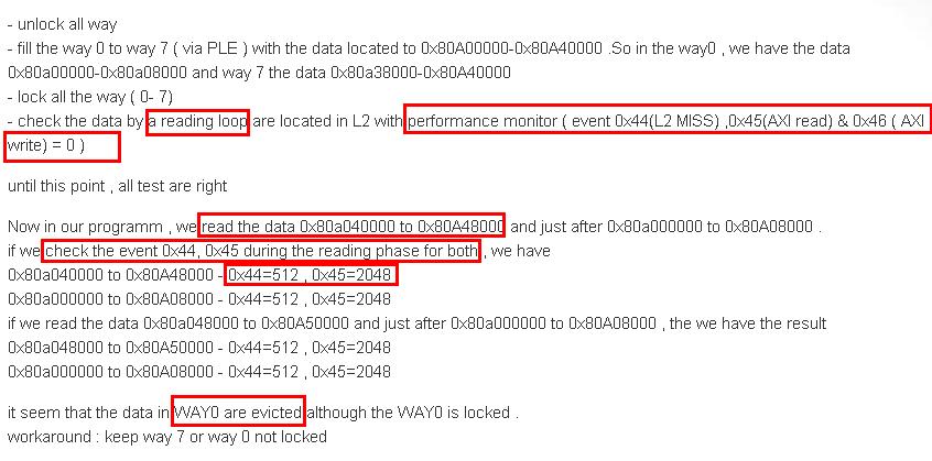
Therefore, I assume once I lock an buffer array on way 0 for example, I can simply access the buffer

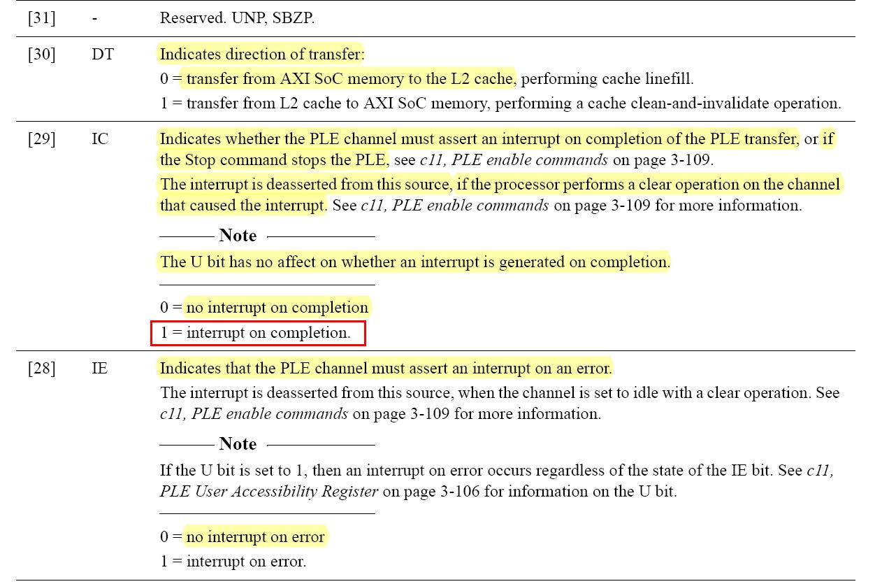
address (or pointer to an array). The CPU would first check way 0 for availability, and if the data has a

cache hit, the AXI read (0x45) would increase; otherwise, the L2 miss (0x44) would increase.  Is my 

statement correct? If the answer is a yes, how could I check the events while read the array data?

Could someone provide a pseudo code for this ?

Thank you in advance,

Joey from Altek

  • Can you specify what is the processor you are using?

  • Hi, Biser:

    Sorry that I did not include my platform info.

    My platform info: TMS320DM8148 (Vision-Mid) 

    600-MHz ARM® Cortex™-A8 RISC MPU

    500-MHz C674x™ VLIW DSP

    200-MHz M3-ISS/M3-HDVPSS 

    BIOS: avsdk_00_08_00_00 (sys-bios)

    Thank you so much for your quick response.

    Regards,

    Joey from Altek

  • There is a dedicated forum for DM8148. I will move your post there.

  • Joey,

    I can find that the Cortex-A8 ARM L2 cache, lock down and PLE are explained in the ARM TRM:

    http://infocenter.arm.com/help/topic/com.arm.doc.ddi0344k/DDI0344K_cortex_a8_r3p2_trm.pdf

    Regards,
    Pavel

  • Hi, Pavel:

    Thank you for your responds.

    I applied the PLE, lock down registers already according to the r3p2 spec, and now I am reading back the data.

    I have no experience on using the cache data before. I searched the spec, but I don't see where it has indicated how to

    read locked data.  My guess is that once I put data in cache, I just have to access the array address, and CPU will

    check the cache for me. Can you tell me if I am correct or can you help pinpoint where I can find the answer in the

    spec.  If my statement is right, how can I prove data is read from cache, not from RAM?

    Thank you,

    joey from altek


  • Joey,

    This looks to be ARM related, so I would recommend you to check with ARM (ask in the ARM forum). Meanwhile I will try to find some answers for you. I will come back to you if I find something useful.

    Regards,
    Pavel

  • Joey,

    Below is some info for the OMAP35x PLE, which should be applicable here:

    It turns out, the OMAP3 DMA can only DMA between DDR and memory addresses in L3/L4 memory space.  Therefore there is no way to use the DMA to get large blocks from DDR into the ARM L2 Cache using the DMA on the ARM side since the L2 cache is not memory mapped.

    The ARM Cortex A8, however, does have capability to do DMA transfers between the L2 Cache and DDR via it's Pre-Load Engine (PLE).

    The L2 PLE has two channels to permit two blocks of data movement to or from the L2 cache RAM.

    Here is some code from ARM Ltd. to program the PLE

    I don't have a C example - as the code uses CP15 instructions intensively. Here is an assembler implementation.

    MOV r0, #1 ; enable user mode to access the PLE

    CP15 registers

    MCR p15, 0, r0, c11, c1, 0 ; write to the PLE User Accessibility Register

    MOV r0, #0 ; select PLE channel 0

    MCR p15, 0, r0, c11, c2, 0 ; write to the PLE Channel Number Register

    MOV r0, #0 ; transfer from memory to L2 and

    transfer data to way 0

    MCR p15, 0, r0, c11, c4, 0 ; write to the PLE Control Register

    LDR r0,=0xF0000000 ; set transfer start address as

    0xF0000000

    MCR p15, 0, r0, c11, c5, 0 ; write to the PLE Internal Start Address Register

    LDR r0,=0x100

    MOV r0, r0, LSL #6 ; transfer 256 lines of data

    MCR p15, 0, r0, c11, c7, 0 ; write to the PLE Internal End Address Register

    MCR p15, 0, r0, c11, c3, 1 ; start PLE enable command Loop

    MRC p15, 0, r0, c11, c8, 0 ; read the PLE Channel Status Register

    TST r0, #3 ; check to see whether the transfer is

    complete

    BNE Loop ; re-read the status register if

    transfer not complete

    MCR p15, 0, r0, c11, c3, 0 ; stop PLE enable command

    Below are also some e2e threads that might be in help:

    http://e2e.ti.com/support/omap/f/849/t/117680.aspx

    http://e2e.ti.com/support/dsp/omap_applications_processors/f/447/t/107835.aspx

    Regards,
    Pavel


  • Joey,

    Here is some feedback from the MPU team:

    For CortexA8 it is possible to lock down cache.  As I recall there are some CP15 registers which allow locking. ARM defined a couple different procedure over time.  A8-L2 uses lockdown format C.  See attached excerpt from ARM Arch manual.

    0741.DDI0406_exerpt_lockdown.pdf

    Back in ARMv4/5/6 in smaller systems it was not uncommon for cache and tlb locking to happen.  In larger systems since then I’ve seen less usage.  Trustzone security in ARMv7 made some of the services not as easily usable and the larger CPUs were more used at HLOS (linux/windows) systems running large software.  Locking was more associated with small RT code and sometimes bug work arounds.   

    ARM does provide hit/miss counters for L1 & L2 interfaces which probably could be used to see if reads are hitting in cache for a controlled loop.   Code execution can be timed and shown much faster when in cache, but given nature of cache allocation, code which is close in time or space tends to be in the cache anyway.  The point of locking is to be predictable so not even a ‘cache warm’ up time is needed (1st time through loop where things enter the cache).
     
    For bigger CortexA class ARMs the need to lock cache is much less for the class of applications which these CPUs target.  Without care and a big system picture, cache locking can hurt the average performance of the bigger system.  For most applications there are other and better ways to speed them up compared to locking.

    Regards,
    Pavel


  • Joey Lin said:

    I searched the spec, but I don't see where it has indicated how to

    read locked data.  My guess is that once I put data in cache, I just have to access the array address, and CPU will

    check the cache for me.

    Yes, locked cache entries work the same as normal unlocked cache entries.  The only difference is that locking ensures it cannot be evicted (except by explicit cache maintainance operations).

    Joey Lin said:
    If my statement is right, how can I prove data is read from cache, not from RAM?

    There are many ways to detect whether an access is hitting cache or not.  A side-effect of caching is loss of coherency:  once a line is in cache, changes made by other masters will not be noticed by the cortex-a8, reads will continue to return the same cached data.  You can test this by attempting to load a cache line (by accessing it or using the PLE) and then modifying memory through DMA or via JTAG (though DAP or any core other than the cortex-a8).

    For write-back cacheable memory regions you get similar behaviour on writes:  a write performed by the cortex-a8 would end up in cache and remain invisible to other masters until the cache line is evicted.

    An alternative approach has already been mentioned above: configure the performance counters to measure various statistics on cache activity.

    If cache doesn't seem to be working, then some things to check:

    • Are bit 0 (MMU enabled) and bit 2 (data caching enabled) set in the control register?
    • Is bit 2 (L2EN) set in the auxiliary control register?
    • Is your memory region configured as cacheable and non-shareable?

    Note that if the MMU is disabled then all memory regions are considered "strongly-ordered" and PLE operations will "complete" instantly without doing anything.

  • Hi, Matthijs:

    Sorry for my late replying. Your feedback is very clear to my questions. I have used the performance

    counter to check cache hit (Write USEREN Register 0x1, Write EVTSEL Register 0x45and Write PMNXSEL Register

    0x0) by checking PMCNT Register (MRC p15, 0, r0, c9, c13, 2).

    After I access the buffer address, I checked PMCNT , but I got 0 count.

    I checked the control register,  bit 0 (MMU is enabled) and bit2 (data caching is enabled) 

    I also checked auxiliary control register, bit 2 (L2EN) is enabled as well.

    My question is how could I check and set memory region as cacheable and non-shareable?

    Currently status. I have studied c10, Memory Region Remap Registers parts, but I still have no idea how to configure

    primary region and normal memory remap register.  However, I do have set control CP15 TRE bit, according 

    the table below. 

    Best regards,

    Joey from Altek


  • The memory remap registers are configured *before* the MMU is enabled since they determine how the MMU interprets the translation descriptors.

    I'm getting the impression that you're saying TRE was already set and the MMU already enabled, and not because you did so?  That would mean you're running under an operating system or at least in some environment where MMU setup has already been taken care of.  If this is indeed the case, then that environment will (or at least should) provide an API to set up memory mappings of the desired type.  Meddling directly with the translation tables (let alone the remap registers) would probably cause problems.

    If my impression is wrong and you do have full authority over the processor configuration then I'll see if I can write up a short how-to on setting up the memory system on the cortex-a8.  I'm currently working on MMU code in my Forth system so all the info I gathered is still fresh in my head.  In my opinion it is actually fairly easy, but it is unnecessarily difficult to gather all the pieces since the TRM omits much info and refers to the architecture ref, but the architecture ref contains lots of info which isn't relevant to the cortex-a8, and also presents all configuration possibilities that were retained for compatibility older architectures, even though the modern way (with TRE and AFE set) is much simpler.

  • Hi, Matthijs:

    Matthijs van Duin said:
    I'm getting the impression that you're saying TRE was already set and the MMU already enabled, and not because you did so?  That would mean you're running under an operating system or at least in some environment where MMU setup has already been taken care of.  If this is indeed the case, then that environment will (or at least should) provide an API to set up memory mappings of the desired type.  Meddling directly with the translation tables (let alone the remap registers) would probably cause problems.

    Sorry for the misunderstanding, the M bit (MMU enable) was already set, but the TRE was not. That was why I followed the table attached in the previous message, and set memory access controlled by remap MMU.  

    Matthijs van Duin said:
    If my impression is wrong and you do have full authority over the processor configuration then I'll see if I can write up a short how-to on setting up the memory system on the cortex-a8.

     Since I am not the 1st person working on this matter before, there are chances that I may accidentally screw up the a8 memory system.  It will be really appreciated if a how-to setting up can be provided in your convenience. 

    Best regards,

    joey from altek

  • Joey Lin said:
    Sorry for the misunderstanding, the M bit (MMU enable) was already set, but the TRE was not.

    This still means that some software has already taken responsibility for creating a translation table and setting up the MMU.  You therefore can't just go edit things: especially altering memory type mapping will affect the behaviour of all existing memory ranges, including the one your code is running from and those for peripherals.  If for example the altered memory type mapping makes peripheral ranges cacheable, needless to say, funny things will happen...

    Normally it should be obvious what code is responsible for MMU, namely the kernel.  If in your case it's not obvious, you'll need to go looking for it.

    (The fact that it doesn't also enable TRE suggests the code was originally written for older arm11 processors, or is explicitly trying to remain compatible with them.)

  • Hi, Matthijs :

    I  checked the a8_app.cfg, and there are settings of mmu for different memory regions.


    5305.a8_app.cfg


    It seems to me that the A8 code/data has been set to be cacheable/no-shareable.

    I checked the number of loops that it needs to take the completion of copy (0x3) from PLE Status Register:

    while(!((status&0x3)==0x3))
    {
            status = Read_PLEStatusRegister(); //p.194
             vcnt++;
    }
    printf("..status 0x%x: loop %d times\n",(UINT32)status, vcnt);

    and it did take some loops to complete the data copying.

    frame 1.

    [CortexA8] ..status 0x3: loop 629 times 

    frame 2.

    [CortexA8] ..status 0x3: loop 95 times

    frame 3.

    [CortexA8] ..status 0x3: loop 79 times

    But the cache read event (0x45) still get 0 count, after accessing the buffer.

    Then I started to wonder maybe my use of PMCNT register for cache hit was not correct. Therefore, I tried to

    check the time differences of  data accessing between with and without applying data locking.  I used memcpy()

    to copy data buffer to a destination buffer repeatedly for 10 times and checked copy time consumption.   If the data

    buffer does lock in L2, and CPU get a cache hit to it, I should be able to see dramatic low time consumption, comparing

    to the one without perform a data lock.  Unfortunately, there seem not much differences between these two cases. The

    result agrees to PMCNT register, which returns cache hit count 0.

    Is there anything else that I need to consider of?

    Best regards,

    joey from altek

  • Ah, so SYS/BIOS is responsible for the MMU setup.  I'm not terribly familiar with SYS/BIOS, but I took a quick look at the ti/sysbios/family/arm/a8/Mmu.* code and it seems to have very little added value:

    • It just seems to do a one-off MMU configuration rather than any sort of active management, and you basically have to dictate the raw MMU settings to it.
    • You can only dictate a very limited subset of MMU settings to it.  In particular, it gives you woefully inadequate control over cacheability.  None of the new functionality introduced in VMSAv7 is supported.  (On the other hand, it does give you the option to specify the 'shareable' attribute which is of very little use on the cortex-a8, and the 'IMP'-bit which is unused on the cortex-a8 and should be zero.)
    • It does have functions to alter mappings at runtime, but to do so it first completely disables the MMU and flushes all caches (!!!) before updating the entry and reenabling the MMU.  While it's busy flushing all the caches, interrupts are disabled.

    I'll try to explain more about the MMU when I have some time, but for now it may be useful to understand how the settings that SYS/BIOS asks for (which uses the archaic cacheable/bufferable terms) impact the memory type on the cortex-a8:

    shareable cacheable bufferable
    (ignored) false false Strongly-ordered
    (ignored) false true Device, shareable
    true true (ignored) Normal, L1 non-cacheable, L2 non-cacheable, shareable
    false true false Normal, L1 write-through, L2 write-through
    false true true Normal, L1 write-back, L2 write-back (no write-allocate)

    But the cache read event (0x45) still get 0 count, after accessing the buffer.

    Event 0x45 counts AXI reads, those are caused by non-cacheable reads and cache linefills, not by cache hits.

    I used memcpy() to copy data buffer to a destination buffer repeatedly for 10 times and checked copy time consumption. 

    If both buffers are cacheable and fit in cache then after the first time they will be there even if you didn't lock them in cache.  If they don't fit in cache then you also can't lock them there.  If one of the two is non-cacheable then this will completely dominate the cost of copying.  Note that if memory regions used for DMA buffers are marked cacheable then you have to do explicit cache maintainance, either by using the cache maintainance instructions or by using the PLE (which basically acts like an asynchronous version of cache maintainance).

    Cache locking itself is just to make sure one or more cache ways remain reserved for the PLE and other stuff doesn't accidently get allocated in them.  The performance benefit should come from being able to have the PLE preload and evict data while doing CPU processing in parallel, e.g. something like:

  • Ick, I just realized that things are not quite as straightforward since the PLE can only evict a cache line back to its original memory location, and as far as I can see there's no way to allocate a cache line into a locked way other than by loading it using the PLE.  It can still work, but it does mean the source buffers should be reused as destination buffers -- not just in L2 cache but also in memory, which reduces flexibility.  In the example above: after the CPU has written destination buffer 4, its eviction will overwrite source buffer 3 whether you want to or not, since that's where those cache lines were originally loaded from.

    It would have been nice if the PLE were a bit more flexible, or if a DMA controller could directly access the A8's L2 cache to deliver data on its doorstep so to speak.  (I guess that might be one of the reasons why TI uses ARM9 cores in the HDVICP subsystem which do have a slave port to allow a DMA controller direct access to their Tightly Coupled Memory.)

  • Hi, Pavel:

    Thank you for your posting.

    I have tried the assembly code you posted here.  Some compilation errors occur, so I assumed the code

    was not originally written for TI compiler.  I made some minor modification to build this code successfully. 

    something I need to clarify with you below:

    1. 

    Pavel Botev said:

    MOV r0, #0 ; transfer from memory to L2 and

    transfer data to way 0

    MCR p15, 0, r0, c11, c4, 0 ; write to the PLE Control Register

    The PLE control register is set as 0x0. Why is the IC bit[29] ignored? Don't you need

    the interrupt to trigger the completion flag?


    2.

    Pavel Botev said:

    LDR r0,=0xF0000000 ; set transfer start address as

    0xF0000000

    Is the start address here an example of any virtual address (ex. mmu re-mapped address)?

    Is there any constraint for this start address? By reading back the start address, I learnt that

    there is always an offset result in the address I have written.

  • Joey,

    This assembly sample code is for OMAP35x device (which is also Cortex-A8 ARM based), http://www.ti.com/product/OMAP3530, thus you should align it with the DM814x device.

    This assembly sample code come directly from ARM. So I would recommend you to check this with ARM.

    Regards,
    Pavel

  • Joey Lin said:

    The PLE control register is set as 0x0. Why is the IC bit[29] ignored? Don't you need the interrupt to trigger the completion flag?

    Since the Cortex-A8 does not have an integrated interrupt controller, the various interrupts it can generate are exported on the CPU boundary and it is up to the system integrator to connect these to some interrupt controller.  As far as I know, the PLE interrupts are not connected to anything on the dm814x, so there is no point in enabling them.  You need to poll for completion.

    Joey Lin said:

    Is the start address here an example of any virtual address (ex. mmu re-mapped address)?  Is there any constraint for this start address? By reading back the start address, I learnt that  there is always an offset result in the address I have written.

    The start address is any virtual address aligned to the cache line size, which is 64 bytes.  When reading back the address, the bottom 6 bits are unpredictable according to the TRM, hence these should officially be masked off (although they always seem to be zero as far as I can tell).  After having run and stopped again, the address is updated with the next address to be transferred.  If it stopped due to an error, this is the faulty address + 64.  If it stopped due to completion, this is the address just past the transferred region.

    The PLE "End Address Register", despite its name, actually contains the length to be transferred, not an address.  The length must likewise be a multiple of the cache line size.  The maximum length that can be transferred is one cache line less than the size of a cache way, which on the DM814x is 512/8 = 64 KB.  After stopping the PLE it is updated with the remaining length to be transferred, i.e. 0 unless the transfer was aborted.

    Keep in mind that that the physical address modulo cache way size (i.e. the bottom 16 bits of the address) determines the cache set for that address.  Together with the chosen cache way, this fully determines where into cache the data is loaded, and anything else that's already there will be evicted first.  This means that if you want to preload data from two different addresses whose bottom 16 bits are the same, you will have to use two different cache ways.

  • Matthijs van Duin said:
    The PLE "End Address Register", despite its name, actually contains the length to be transferred, not an address.  The length must likewise be a multiple of the cache line size.  The maximum length that can be transferred is one cache line less than the size of a cache way

    Correction, based on testing it appears that the register contains the length to be transferred minus one cache line, so programming it with 0 means 64 bytes will be transferred, while programming it with 0xFFC0 will transfer the full 64 KB of the selected cache way (assuming flat or otherwise unproblematic MMU mapping).  This makes more sense, but the documentation could really use some improvement here...

    Note btw that if you aim for portability you cannot assume the L2 cache way size is 64 KB.  Based on browsing some datasheets, the 512 KB of L2 cache available on dm814x is unusual:  all of the closely related devices (dm816x, dm38x, am335x) only have 256 KB of L2 cache, which means 32 KB per cache way.

  • Matthijs van Duin said:
    If it stopped due to an error, this is the faulty address + 64.

    Sorry, this is wrong.  The documentation says "The address where the fault occurred is captured in the L2 PLE Internal Start Address Register".  This appears correct in case of an MMU fault.  In case of an external fault, the address seems to be the fault address + 3*64, at least for preloading, but I don't know if this can be relied on.

  • Hi, Matthijs:

    Matthijs van Duin said:
    The start address is any virtual address aligned to the cache line size, which is 64 bytes.

    How would you handle start address alignment issue, if the address is not multiple of 64?  Unlike data alignment, data padding would not apply in this case, right?

    Matthijs van Duin said:
    When reading back the address, the bottom 6 bits are unpredictable according to the TRM, hence these should officially be masked off (although they always seem to be zero as far as I can tell).

    Okey.., if the bottom 6 bits are unpredictable, can we assume the address is written correctly? Just out of curiosity, why an unpredictable interface is provided for?

    Best regards,

    Joey from Altek    

  • Joey Lin said:
    How would you handle start address alignment issue, if the address is not multiple of 64?  Unlike data alignment, data padding would not apply in this case, right?

    I'm not sure what you mean.  Given that the address range is just used for cache management, typically you would simply round the start address down and the end address up to the nearest cache line boundary.  If a few extra bytes get preloaded and evicted again that's normally not a problem.  The only restriction to keep in mind is that when "ownership" of memory is being passed around from core to core, or between core and a DMA controller, this must also happen at cacheline boundaries.

    Joey Lin said:
    Okey.., if the bottom 6 bits are unpredictable, can we assume the address is written correctly?

    Since PLE only works with 64-byte aligned addresses, clearing the bottom 6 bits of the value you read from the "start address" register will give you the actual address.  Before you start the PLE this should match the address you wrote to it (since it should be aligned also), after the PLE has completed it should be equal to start_address + length.  (I mean actual transfer length here, i.e. 64 + the value programmed into the PLE's poorly named "end address" register.)

    Joey Lin said:
    Just out of curiosity, why an unpredictable interface is provided for?

    My impression is that those 6 bits are actually "RAZ/WI" (reads as zero, write ignored), but often such bits are declared "UNP/SBZP" (reads unpredictable, writes should be zero or preserve the last value read) to allow ARM some flexibility without risking software incompatibility.  For example, an (older or newer) implementation might allow those bits to actually reflect the value last written (even if otherwise ignored), or they could be used for some other purpose.