Hello,
My customer is testing the C6678 TSIP interface via external loopback on a prototype board. They have a 8.192 MHz single data rate serial clock and a 8 KHz serial frame sync as inputs to the C6678. They have modified the TSIP_testProject found in pdk_C6678_1_1_2_6 accordingly. They have placed the C6678 into LLB mode and generate a test tone on TSIP0_TR00 and monitor TSIP0_TX00 for the loopback tone. However, Section 5.1.3.3, LLB Testing, of the Telecom Serial Interface Port User Guide (sprugy4.pdf) states that:
"Successful operation is determined by comparing the transmit serial links with a delayed version of the receive serial links.”
Questions:
1) Is this delay quantified elsewhere in the User Guide?
2) Where are the registers for DX0/DR0 and SX0/SR0 located to determine if the transmit serial output is equivalent to the receive serial input?
3) To clarify, what are the addresses that can be compared in the Code Composer Memory Browser to confirm that the input and output match?
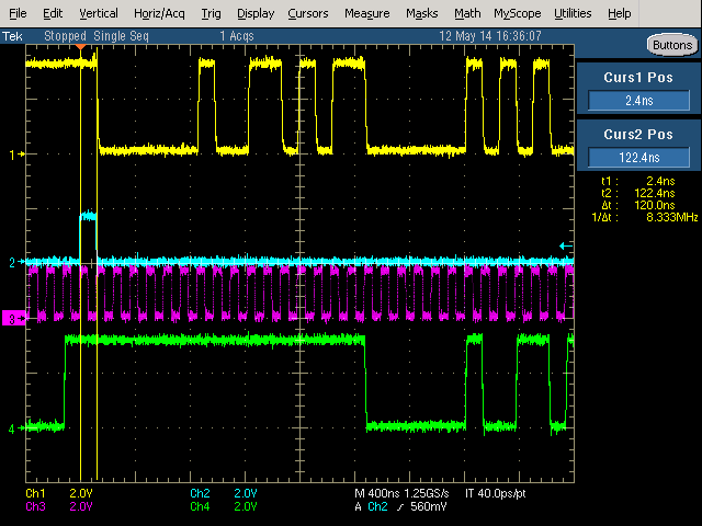
The oscilloscope capture appears to verify that LLB mode loopback is successful, but they would like to verify this through memory/register inspection.
I've attached an oscilloscope capture as detailed below:
Signal 1: TSIP0_TR00
Signal 2: TSIP0_FSA0
Signal 3: TSIP0_CLKA0
Signal 4: TSIP0_TX00
Thank you for your help!
Electrons4me