This thread has been locked.

If you have a related question, please click the "Ask a related question" button in the top right corner. The newly created question will be automatically linked to this question.

DDR3 routing constraints for write-leveling on C6670 EVM

Expert 2985 points

Hi all, 

When I read the DDR3 Design Requirements for KeyStone Devices(SPRABI1B), I am confused about some details.

So I want to show my understanding about these and ask you help me to confirm whether my understanding is right or not.

**************************************************************************************************

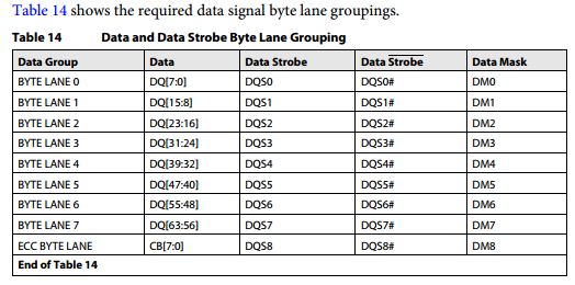
From what I understood, according to this pic below

(1) when the Invert clock out state is disabled and DDR3 runs at 1333MT/s

2.027 inchs < addr/cmd/ctl length - data length < 11.861

(2) when the Invert clock out state is enabled and DDR3 runs at 1333MT/s

-2.138 inchs < addr/cmd/ctl length - data length < 7.694

Am I right?

If it is true, I think this constraint is too generous when the Invert clock out state is enabled!

**************************************************************************************************

In the C6670 EVM board, the layout engineer sets the constraint about the skew between addr/cmd/ctl length and data length showed in the pic below

the U18 is the first DRAM on the fly-by topology and the others are U19, U21,U22.

From what I understand, to a given DRAM, the skews between the CLK length to it and the DQS length to it should be concerned.

But why constrain the skews between the CLK length to the first DRAM and the DQS length to every DRAM according to the pic above?

**************************************************************************************************

That's my question. Hope anyone help me.

Regards,

Feng

  • Hi Feng,

    As you stated, the address/command/clock signals are constrained to ensure that these lengths are very closely matched and the signals for each data lane are constrained so that they are very closely matched. The constraint between the address/command/clock signals and each of the data lanes is necessary for successful leveling. The constraints you labeled (1) and (2) above are accurate. The designer of the C6670 set the constrains tighter than the targets in the DDR3 Design Requirements for KeyStone Devices(SPRABI1B). 

    Regards, Bill

  • Hi Bill,

    Thanks for you reply!

    So for a given DRAM why does the EVM constrain the skews between the data length to this DRAM and the DQS length to the first DRAM?

    Why not constrain the skews between the data length to it and the DQS length to it  for a given DRAM?

    Is it just for the purpose that it make the constraint tighter? But it confuses who see this.


    Regards,

    Feng

  • Hi Feng,

    Multiple sets of constraints exist for the DDR3 routing. There is a constraint on the length differential for each of the signals in a byte lane which includes the DQS, the DQM and the data signals as shown in the table below. This is described in section 4.3.1.6. There is also a constraint on the length differential for the address, command and clock signals from the C6670 to each of the DDR3 memories as described in section 4.3.1.4. Note that the length of these signals to each memory in the fly-by chain will increase. There is also the  constraint which you are asking about that defines the length differential between the data byte lane and the address/command/clock signals. This final constraint is needed to ensure that the C6670 can properly level the accesses for each byte lane. All three constraints must be met for proper operation of your DDR3 interface.

    Regards, Bill 

  • Bill, I am appreciated for your patience to answer my question.

    As you mentioned above,

    " There is also the constraint which you are asking about that defines the length differential between the data byte lane and the address/command/clock signals. "

    For a given DRAM,  I think "the length differential between the data byte lane and the address/command/clock signals" means the CLK length from DSP to this DRAM subtracts the DQS length from DSP to the same DRAM.

    Am I right?


    But what confused me on the EVM is that the layout engineer constrained the the CLK length from DSP to first DRAM substrate the DQS length from DSP to the given DRAM. For example 


    see the second red rectangle, the engineer constrained the skew between the CLK length from DSP1 to U18 and the DQS length from DSP1 to U19. Not the same DRAM.

    I think it doesn't make sense! This confused me!

  • Hi Feng,

    I understand your confusion and I agree that the constraints set by the Advantech designer do not match the wording in the DDR3 Implementation Guide but they achieve the same result. Remember that the skew must be between the minimum and the maximum defined in the implementation guide. The maximum skew is 7.5" to 12" depending on the state of invert clock. Since the board is only 9" wide it is not possible to exceed the maximum so we only have to worry about meeting the minimum skew.

    Advantech chose to define the constraint between the DQS from the C6670 to the associated DDR memory and the clock length to the first memory. Remember that we are mainly concerned about meeting the minimum requirement. The clock is routed in fly-by mode from the C6670 to the first DDR, to the second DDR continuing to each memory and finally to the termination at the end of the chain. Based on this, the clock length will be as follows.

    first memory = length from C6670 to DDR memory for byte lane 0 & 1.

    second memory = length from C6670 to DDR memory for byte lane 0 & 1 + length from first memory to second memory.

    third memory = length from C6670 to DDR memory for byte lane 0 & 1 + length from first memory to second memory + length from second memory to third memory.

    Based on this you can see that the skew between the length of the DQS to a memory chip and the clock from the C6670 to that same memory chip will always be greater than or equal to the skew between the length of that same DQS and the length to the first memory chip.  Therefore the constraint above will always result in trace lengths that meet the minimum skew requirement to all DDR3 memories. 

    I agree that this is a little confusing but it is the method that Advantech chose to use.

    Regards, Bill

  • I got it!

    I am very appreciated for your interpretation with so much details showing the whole thinking way.

    Thank you again!

    Regards,

    Feng