Other Parts Discussed in Thread: AM3874
Hi,
I have one question regarding clock input circuit of AM3874 device.
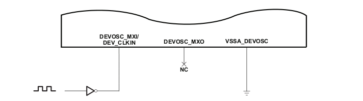
Now my customer uses an oscillator for supplying clock to AM3874.
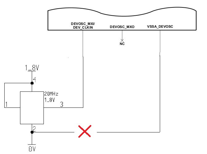
The osc's output is connected to DEV_CLKIN(AH2) pin. And Both GND pin of the osc and VSSA_DEVOSC(AG3) pin are connected to each other, and also osc's gnd pin is connected to Gnd(0V).
Recently, our customer found one oscillator that is not connected to gnd(0V) by failure mounted. However, according to the measurement of clock wave, the waveform of failure mounted is not bad. It was almost same as normal mounted. There was no effect by power line noise.
Do you know the internal circuit of relation of VSSA_DEVOSC and VSS? Customer would like to know whether AM3874 CLOCK INPUT(DEV_OSC) is not influenced from VSSA_DEVOSC pin condition.
Please advise me.
Best regards,
Michi