This thread has been locked.

If you have a related question, please click the "Ask a related question" button in the top right corner. The newly created question will be automatically linked to this question.

Dose DM6437 DDR2 memory controller support a seamless burst write operation?

Hi Champs,

I've got the JEDEC standard JESD79-2B and the standard defines a seamless burst write operation as follows.

  o JEDEC STANDARD DDR2 SDRAM SPECIFICATION JESD79-2B
    (cs.ecs.baylor.edu/~maurer/CSI5338/JESD79-B2.pdf)

    - Page 36

      Figure 33 - Seamless burst write operation: RL = 5, WL = 4, BL = 4

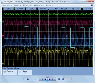
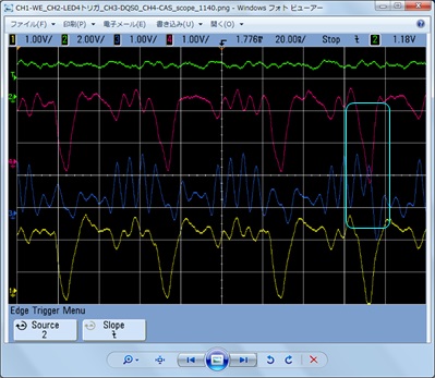
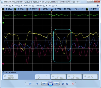
So, dose DM6437 DDR2 memory controller support the seamless burst write operation?

The DM6437 memory controller supports JESD79-2A, but I think that it also defines the operation.

Regards,
j-breeze

  • Hi Champs,

    Dose anyone have any information?
    Any help would be appreciated.

    Regards,
    j-breeze

  • Hi Champs,

    I really need your help.
    Could you please let me know whether DM6437 DDR2 memory controller support the seamless burst write operation or not?

    Regards,
    j-breeze

  • Hi J-Breeze

    The DM6437 EMIF controller is designed to support back to back read/writes, as long as the masters and the system interconnect can sustain it. Other interruptions would be things like bank conflicts and refresh management.

    Typically masters like EDMA are able to do big burst transfers (big ACNT etc) to keep the EMIF bus utilization close to max, other masters might not be able to do so.  We don't have any published EDMA throughput data for the device, but I recollect that with big ACNT (~ 4K) you could accomplish higher than 85% bus utilization. 

    You can look at DM6467 SoC Overview and Throughput application note 

    http://www.ti.com/lit/an/spraaw4b/spraaw4b.pdf

    Although different device, it has similar EMIF and EDMA controller and EDMA throughput data numbers in this application note might provide some guidance.

    Hope this helps.
    Regards

    Mukul 

  • Hi Mukul,


    Thanks for your support.


    So, I'd like to ask you one more question. 

    When I execute a code below on dsp core and there are no other masters, dose the back to back read/writes occur as well? 


        for ( i = ddr_start_address ; i < ddr_end_address ; i += 4 )
        {
            *( volatile Uint32* )i = val;
        }

    I'd appreciate your continued support.


    Regards,
    j-breeze

  • Hi Mukul,

    I'd appreciate it if you could help me.

    When I execute the code that I mentioned previous my post, I'm facing a strange behaviour.
    It seems that the back to back writes sometimes occur and sometimes does not occur.

    So, could you please give me some advice about a cause that can be considered or anything that I should check more? 


    Regards,
    j-breeze

  • Do you have more details on your observations, what do you mean by sometime you are able to get b2b writes vs sometimes not? How much gap are you seeing in working vs non working use-case?

    Can you make sure the down time is not just because of things like  bank conflicts and ddr refresh management.

    Please also note that in a "real" system, there will be more masters in the systems that could be simultaneously accessing DDR , so continuous back to back writes even though supported by the controller might not be realistic - I hope this is understood?


  • Hi Mukul,

    I'm sorry for my late reply and I'd appreciate your advice.

    I've got a wavefrom below measured by one of my customers.  The customer guess it's the b2b writes because the WE signal overlaps with DQS signal that you can see in blue boxes on the waveform.  The customer thinks it corresponds to the seamless burst write operation in the JEDEC standard.

    It seems the insufficient information though I'd like your opinions about the waveform.

    Would you think that it's the b2b writes?  Any comments would be appreciated.

    o Figure 1. Measured Waveform


      Yellow : WE 
      Blue   : DQS
      Red    : CAS

    o Figure 2. Enlarged a blue box in the Figure 1


      Yellow : WE 
      Blue   : DQS
      Red    : CAS

    o Figure 3. Enlarged a blue box in the Figure 1 (with CK instead of CAS)


      Yellow : WE 

      Blue   : DQS
      Red    : CK

    Regards,
    j-breeze

  • j-breeze,

    I cannot draw any conclusions from the scope captures.  The signal integrity is marginal either due to the PCB layout or the scope bandwidth.  Can you capture the same problem at a lower DDR data rate to make the timing more clear?  The problem should still exist at lower rates.  What data rate are you running?

    What is the problem being flagged?  Are they concerned because they see WRITE Commands in the same clock as when DQS is toggling?  This is not a problem.  The DDR interface as defined by JEDEC operates with pipelined command cycles.  The data portion of the read or write happens several clocks later.  This is defined as the CL delay.  The DDR controller comprehends the pipelined nature of this interface and continues issuing new commands.  This is normal.  Please see Figure 22 from the DDR2 JEDEC spec which shows a back-to-back write.  You can see that the second write command is coincident with the DATA phases of the first write.  Different CL settings or controller delays could move this to second command to match the scope pictures provided.

    Tom

    1541.JEDEC DDR2 JESD79-2C back to back writes.pdf


  • Followup question from email:

    "They want to know in what cases both the DQS & WE are asserted at the same timing.  They guesses this happens during back-to-back writing.  They want to know if their understanding is correct, and also if any other case cause this, they want to know.  The reason why they are asking such very detail is that they are seeing a big difference of boot time between their revisions of application.  And, they think this external RAM access affects to this boot time gap."

    DDR EMIF preformance is not going to impact boot time unless the data rate has been changed significantly.  Boot delay is primarily driven by the bandwidth of the boot interface and the size of the boot image.  I would lokk into these aspects.  You can also profile to previous and current images to understand which parts of the boot process changed.

    Tom