This thread has been locked.

If you have a related question, please click the "Ask a related question" button in the top right corner. The newly created question will be automatically linked to this question.

Using SLAA210A - Getting Started With the Data Converter Plug-In

Other Parts Discussed in Thread: THS1206, THS1206M-EVM

Hi,

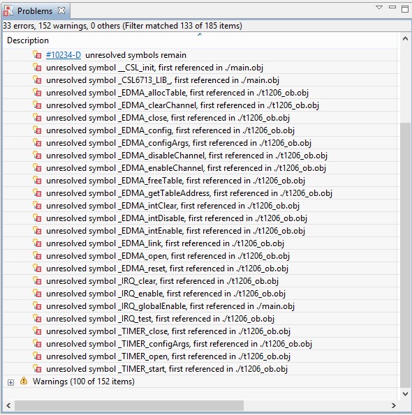
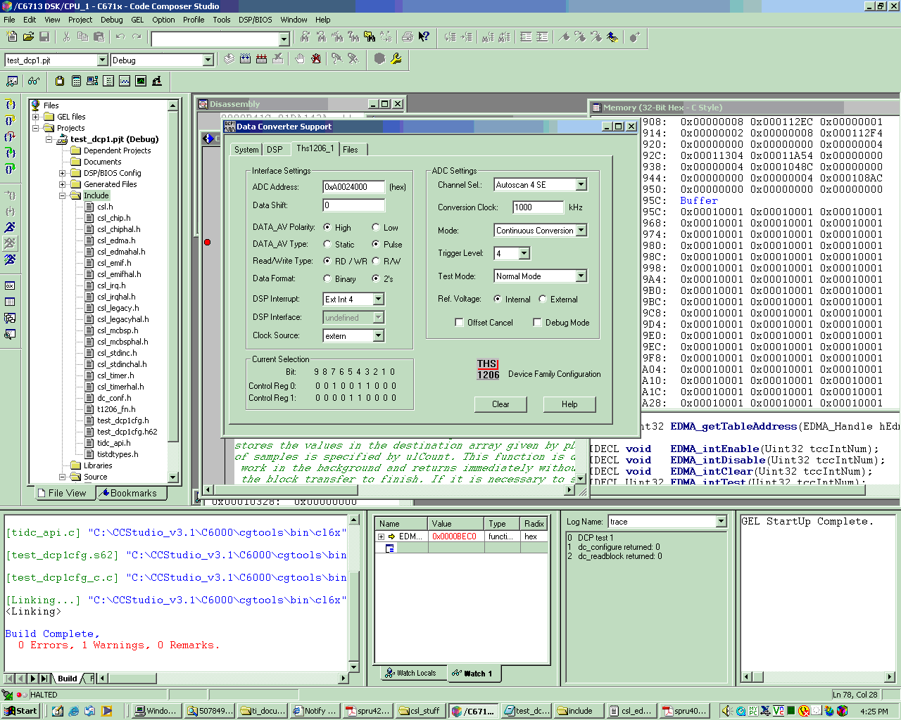
I want to communicate with a THS1206 from a C6713 DSK via a 5-6k interface board, and have tried using the example in SLAA210A.

My question is: how do you determine the ADC Address which should be entered in the Data Converter Support (DCP) tool, which creates the files used in a program to call the functions such as dc_configure(), anddc_readblock()?

SLAA210A shows an ADS Address of 0 in figure 6 found on page 10.

Should it be 0x8000 0000,  0x9000 0000, 0xA000 0000, or 0xB000 0000?

Thanks!

Harry


  • Hello Mr. Thompson,

    please use address 0xA0024000 with the jumper settings important to the address generation:

    5/6K interface board (revB):

    W1: open
    W6: 1-2

    THS1206M-EVM

    W2: closed
    W3: closed
    W4: A

    If you have additional questions please let me know!

    Best regards,
    Lars

  • Hello Mr Lotzenburger,

    Thanks for the information! We have made progress and the analyzer shows we are communicating with the board when dc_configure is called. However, the call to dc_readblock shows minimal activity and I do not see anything being uploaded to my buffer.

    I am concerned over the interface settings being used in the DCP. I am using:

    Interface Settings                                         ADC Settings

    ADC Address - 0xA0024000                      Channel Set:                   Autoscan 4 SE
    Data Shift        - 0                                           Conversion Clock:         1000 kHz
    DATA_AV Polarity - High                              Mode                                 Continuous Conversion
    Data_AV Type       - Pulse                            Trigger Level                    4
    Read/Write Type  - RD/WR                          Test Mode                        Normal Mode
    Data Format         - 2's                                  Ref Voltage                       Internal
    DSP Interrupt       - Ext Int4
    Clock Source       - extern

     The only changes from figure 6 in SLAA210A are the ADC Address, Channel Sel, and Trigger Level

    Please let me know if there is anything in the settings I am missing.

    Thanks!

    Harry


  • Hello Mr. Thompson,

    Looks like you don't get the interrupt from the THS1206. You selected Ext Int 4, but with J13 connected to "b" on the 5/6k I/F you have to select Ext Int 5 in the GUI. The same with the Clock Source for the THS1206. With set to "extern" you need to supply it from an external source. I'd recommend to use Timer 1 first and setting J14  to 3-4 (TOUTb) in this case.

    I attached an example project with your hardware config and CCS3v3. Included in those files you can also find an htm file describing the s/w and h/w settings.
    Just in case there are still problems....

    Please let me know if this solved your problem!

    Best regards,
    Lars

    THS1206-DSK6713-CCS3v3.zip
  • Hi Lars,

    Still having trouble.

    Should bit 5 (that would be 0x0020) in the interrupt enable register be set when your programs are running? I tried the .out files you sent (using CCS 3.1) and it appears bit 5 is not being set.

    Thanks for your assistance!

    Harry


  • Hi Lars,

     **Kevin typing here:

    Lars, our docs say TOUTa goes to timer 1 and TOUTb goes to timer2.  When we connected W14 to 3-4 as you say, the config routine stopped working.  We went back to the 1-2 position and the config worked again.  But our DMA buffer is still not being filled.  It is all 0's.

    end of Kevin's typing****

    Any ideas are welcome!

    Harry

  • Hi Lars,

    I got a program running & receiving information when I use the "analog input AINP" channel select. However, the THS1206 will be reading 4 analog signals, so I will need to use the "Autoscan 4 SE" channel select. When I do this, the values seem skewed.

    Is there anything special I need to consider when using the 4 channel select?

    Could there be a timing issue?

    Thanks!

    Harry

  • Hi Harry,

    nice to hear that you can sample now.
    I'm not aware of any special care abouts in "Autoscan 4 SE", except that bit combination "11" for  TRIG1,0 is not allowed.
    Could you send a screenshot of your graph(s)? I assume you sorted the buffer in 4 sub buffers to deinterlace the channels?!

    Best regards,
    Lars

  • Hi Lars,

    Can you contact me?

    We have discovered the clock on the THS1206 is running at 1KHz, which is way off.

    Thanks for your valuable time,

    Harry Thompson


  • Hi Harry,

    ok, I'll contact you then...

    In the meantime I send you an example project for CCS3v1 I run successfully today.

    Best regards,
    Lars

    THS1206-DSK6713-CCS3v1.zip
  • Dear Lars,

    Thanks for your great help! Everything is working and we have made great progress!

    Cheers,
    Harry Thompson

  • Hi,

    I have run this code in ccsv3.1 successfully and it works great. However, is it possible to get a CCSv5.4 version of either this version of the code or the 3.3v? I tried importing the 3.3 version however I get errors error when I try to debug:

    Any info you could provide on how to get this valuable code to a higher version would be greatly appreciated.

    Sincerely,

    Brady