This thread has been locked.

If you have a related question, please click the "Ask a related question" button in the top right corner. The newly created question will be automatically linked to this question.

66AK2E05 and DRAM

Other Parts Discussed in Thread: 66AK2E05

We currently putting our first 66AK2E05 system into operation. We can already load your custom bootloader via serial interface into the internal RAM, but we have some problems putting DRAM into operation, some support from your side is highly appreciated, because the behaviour of the 66AK2E05 looks a bit strange.

We checked electrical properties (voltages, reset sequence, DRAM clock 667 MHz, etc.), everything looks fine. DRAM configuration is one bank with 2 GB, 4 x 4 Gbit DDR3L-1600, no ECC.

The status register PGSR0 has a strange behaviour:

After reseting PGSR0 contains 0xb000001f. According to data sheet, bits 28-30 must be 0, so this is behaviour is not according to your specification. After DRAM initialization bit 30 and 28 are still set and DRAM is not working.

Can you help us with this point? We currently stuck here and have no concrete idea how to proceed. Any help is highly appreciated.

  • New information.

    After DDR-Phy reset we get PGSRO = 0x0.

    After initialisation we get PGSRO = 0xb1c001ff. This mean we get Read Bit Deskew error, write leveling adjustment error and DQS gate training error.

  • Hello,

    I hope anyone can help me.

    I get leveling erros PGSR0 = 0xB1C001FF. I use following DDR3 chips MT41K256M16. I use four chips in one rank configuration with no ECC.

    I disabled  DATX8_8 because I have no ECC. 

    I have following configuration in u-boot:

    static struct ddr3_phy_config ddr3phy_1600_64 = {
        .pllcr        = 0x0001C000ul,
        .pgcr1_mask    = (IODDRM_MASK | ZCKSEL_MASK),
        .pgcr1_val    = ((1 << 2) | (1 << 7) | (1 << 23)),
        .ptr0        = 0x42C21590ul,
        .ptr1        = 0xD05612C0ul,
        .ptr2        = 0, /* not set in gel */
        .ptr3        = 0x08861A80ul,
        .ptr4        = 0x0C827100ul,
        .dcr_mask    = (PDQ_MASK | MPRDQ_MASK | BYTEMASK_MASK),
        .dcr_val    = ((1 << 10)),
        .dtpr0        = 0x9D9CBB66ul,
        .dtpr1        = 0x12840300ul,
        .dtpr2        = 0x5002D200ul,
        .mr0        = 0x00001C70ul,
        .mr1        = 0x00000006ul,
        .mr2        = 0x00000018ul,
        .dtcr        = 0x710035C7ul,
        .pgcr2        = 0x00F07A12ul,
        .zq0cr1        = 0x0001005Dul,
        .zq1cr1        = 0x0001005Bul,
        .zq2cr1        = 0x0001005Bul,
        .pir_v1        = 0x00000033ul,
        .pir_v2        = 0x0000FF81ul,
    };

    static struct ddr3_emif_config ddr3_1600_64 = {
        .sdcfg        = 0x62000E63ul, //CWL = 5
        .sdtim1        = 0x166C9855ul,
        .sdtim2        = 0x00001D4Aul,
        .sdtim3        = 0x421DFF53ul,
        .sdtim4        = 0x543F07FFul,
        .zqcfg        = 0x50073200ul,
        .sdrfc        = 0x00001869ul,
    };

    For testing I disabled all data bytes and the PGSR0 shows 0xB18001FF in normal clock mode. In invert clock mode PGSR0 shows 0xB10001FF.

    In normal clock mode. If I only enable Byte 0-1 I get PGSR0 = 0xB1C0001FF. If I only enable Byte 2-3/4-5/6-7 I get PGSR0 = 0xB18001FF.

  • Debugging this at the UBOOT level is too difficult.  I recommend that you initially get your board working by use of a GEL file using CCS.  Once this is functional, then porting the configuration changes into uboot is reasonable.

    The DDR3 Controller and PHY on the K2E have several registers that must be properly configured to match the SDRAM timing and the implemented topology.  The bit definitions for these registers are listed in the KeyStone II DDR3 Controller User Guide (SPRUHN7).  I have attached a spreadsheet tool that provides additional guidance calculating the appropriate registers.  (This is a pre-release of this spreadsheet that will be released on the K2E product page in the near future.)  Please fill it out and attach your variant containing the values for your design.

    5037.K2 DDR3 Register Calc v1p50.xlsx

    DDR3 memory systems will only function properly if the ADDR/CMD/CNTRL/CLK signals are routed properly in a fly-by topology.  Also, these fly-by routes and the point-to-point data routes must be properly length matched.  This is discussed in the KeyStone DDR3 Design Requirements (SPRABI1).  Please provide a block diagram showing your layout topology and post a report showing that the routing rules are met.  A sample report is attached below:

    2308.Shn_EVM_DDR3_Rules_1201.xls

    Tom

  • Team,

    thanks a lot, customer found the issue, it was related to PCB, and comments above helped them to find the issue.,

  • Hi,

    Would it be possible to post more information on the resolution to this problem please, or maybe PM if preferred?

    We are seeing exactly the same issue on a 66AK2E05 custom board. No matter how we configure DDR3A, PGSR0 always contains 0xB1C001FF after initialisation.

    The initialisation code we're using for testing is basically the GEL file for the K2E EVM converted to C, loaded and executed using a JTAG debugger. We have used the latest spreadsheet to replace the register settings with values suitable for our board.

    Any help would be much appreciated.
    Thanks

  • The value reported by the PGSR0 register indicates leveling failure.  This is most likely due to improper layout.  Previously in this thread a template was provided showing how to verify that the length matching rules are met.  Please provide an equivalent report showing that the routing rules have been met.  The fly-by nets must be routed as a group and properly length matched from the SOC to each SDRAM in turn.  Data group nets are point-to-point and must be routed as a group for each byte lane.  Please show this in your report.

    Leveling failure can also be due to improper connections between the SOC and SDRAMs.  This can be verified in the schematic. You cannot swap any address, command, control or clock nets.

    Tom


  • Hi Tom,

    Sorry for the delay getting back to you. We're putting together some information regarding our layout etc, but is it possible we could send it to you directly, e.g. via PM or email, rather than post on a public forum?

    Thanks
  • Craig,

    We cannot perform a detailed layout review.  You need to follow the rules and complete the templates showing that the routing rules have been followed.  We can review these reports and provide suggestions.

    The KeyStone I and II EVM designs also contain DDR layout examples.

    Tom


  • Thanks Tom.

    The attached spreadsheet should be in the format you've requested, showing that the routing rules have been followed, and we've included screenshots of the layout alongside the data.

    DDR3 Length Matching Report.xls

  • Craig,

    The fly-by connections between the DDR3 Controller/PHY and the first SDRAM is unusual.  There are 4 nets that route over to the left from the others.  The image is not clear.  Do these nets connect to the second SDRAM prior to connecting to the first one?  If so, this is not acceptable.  They must connect to the SDRAMs in teh same order.

    I also see where some routes appear to cross a keep-out area near a hole in the board.  All DDR3 routes must be adjacent to a solid reference plane.  They must not cross and plane splits or voids.

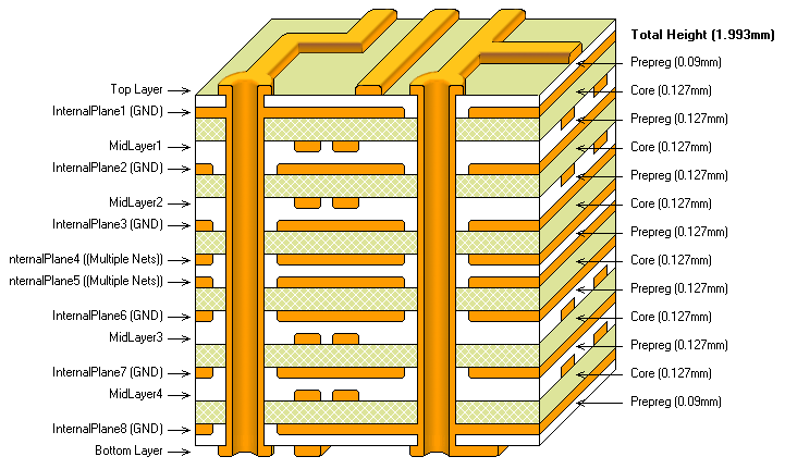
    Please provide a stackup for the board showing the DDR routing layers and the reference planes for each.  Data group routes must have a solid ground reference plane.  Fly-by (address, command, control and clock) must be referenced to either solid ground or solid DVDD15 planes.  If using DVDD15, decoupling must be placed near each end of the routes to provide a low impedance AC return path.

    The data group nets are routed close for proper matching.  It appears that some routes within a group are routed on different layers.  We recommend keeping all 11 nets for each data group on the same layer to simply length matching.  This allows you to ignore the vis barrel length.

    The length matching for the Clock, Address, Command and Control nets is not complete.  These must be routed in a fly-by configuration.  Then the routes must be length matched for each segment. Even though you assert that the routes from SDRAM to SDRAM are same, please provide the lengths for these connections.  It is easy to not realize accumulating error in fly-by layouts due to the stubs.  For instance, lets assume the fly-by connections are:
    DSP -> SDRAM1 -> SDRAM2 -> SDRAM3 -> SDRAM4 -> VTT_terminations
    Then the length matching must show the rule are met for:
    DSP -> SDRAM1
    DSP -> SDRAM2
    DSP -> SDRAM3
    DSP -> SDRAM4
    Please provide this information.

    Tom


  • Hi Tom,


    I can answer some of these.All of the fly-by signals do indeed get routed to the right-most device first, so the ordering is correct. It's not absolutely ideal, since most of the signals go through one extra via to the right of this device, but a few signals go directly to the break-out vias of it. I didn't see this as much of an issue though since we're not intending to run this memory very fast. 400MHz (800Mbps) would be plenty.

    The stack-up is as shown here:

    All DDR3 signalling is done through Mid-layers 1-4 which all have a solid ground plane above and below them. All of the power planes are squeezed into the middle two split planes. I've checked the continuity of every signal's return path ensuring that there are enough GND vias close to all layer transitions, so this shouldn't be an issue.

    I couldn't quite break out all the signals of each data group on the same layer, so the via barrels will incur a slight length-matching discrepancy on the odd signals. I think the worst case is 20mils (0.2% of a bit-length@800Mbps). Unfortunately, our layout software isn't clever enough to take barrel lengths into account, but I thought this amount of skew would be negligible.

    As for the segment length matching between devices, again our software doesn't really make this easy to do. I did provide net-ties at the last device so that the tracks between the last device and the terminating resistors was not included in the length-matching. The worst-case cumulative matching error will certainly be less than 1% of a bit-length, so I can't see how this would break anything. I could try to measure all the tracks to get the exact numbers, but it may take a few days.

    The u-boot software that we're trying to run, and the simplified code which Craig has written both fail (complete loss of debug connection) as soon as it tries to access memory at 0x8000 0000, but the data sheet for our device (AM5K2EO5) says that this part of the memory map is reserved. Can you confirm that the DDR3 interface is mapped to 0x8000 0000 and that we don't need to set-up this aliasing in some way before it can be used?

    Also, should it be possible for us to slow the interface down to say 100/200MHz, since this should in theory allow the memory to be used without any read/write leveling being done, as per older DDR2 interfaces?

    Many thanks,

    Richard

  • Richard,

    I agree that the length matching skew issues would be minimized when operating at 800MT/s (400MHz DDR3 CLK).  If you evern intend to increase the data rate, I recommend that you have the layout team properly constrain the layout so that it meets the length matching guidelines.

    That being said, the layout as you described it should be functionally robust at 800MT/s.  There appears to be some other fundamental issue.  I am concerned that it is hidden by your attempts to debug the DDR behavior while using Linux.  We always recommend that the DDR3 implementation be validated using CCS and GEL files.  Then once the board layout and the configuration are known to be robust, then you integrate the Linux environment with the proven configuration.

    Additionally, DDR3 memory is not located at 0x8000_0000.  This location is reserved.  DDR3 memory is located at 0x08_0000_0000.  This is visible from the ARM cores.  However, it is not directly visible from the DSP core of the other SOC masters unless the MPAX is properly configured.  Please refer to the last few lines of Table 6-1 in the K2E Data Manual and the footnotes below it.

    DDR3 devices are not rated for operation below 666MT/s and the DDR3 PHY on K2E is not rated for operation below 800MT/s.  Operation below these rated is not allowed.

    I recommend that you shift your DDR3 validation back to use of CCS the GEL file.  The K2 DDR3 Init App Note is now on-line at: http://www.ti.com/lit/pdf/sprabx7.  The productized K2 REG_CALC spreadsheet can be linked from it.  Please populate a copy of this spreadsheet and post it.

    Tom


  • Hi Tom,


    Thanks for looking into this for us, but it turns out the issue was a bit simpler than we thought. Our code was trying to do the data leveling on all byte lanes including the ECC lane, but we don't have the ECC lane connected, so this was breaking the leveling process. Now that we've disabled leveling on the ECC lane the memory has burst into life and is indeed very robust at 800Mbps.

    Thanks again for your help.

    Richard

  • Richard,

    Glad to hear that you have this resolved.

    Tom