This thread has been locked.

If you have a related question, please click the "Ask a related question" button in the top right corner. The newly created question will be automatically linked to this question.

Unable to boot AM3874 using 16-bit data bus width DDR3

Other Parts Discussed in Thread: AM3874, AM3892, AM3871, AM3894, AM3352

Hi,


We have a new custom board based on AM3874. We had used this CPU before on a different project. Both boards are using U-Boot version based on EZSDK 5.05.02.0.


Here’s the quick info on this new board:


-          CPU is configured for 720MHz and DDR3 runs at 400MHz

-          Will boot from NOR flash

-          Using 1 x Micron MT41K256M16HA-125 DDR3 chip (16-bit data interface, 512MB size) connected to EMIF0

-          EMIF0 is configured for 16-bit data bus width (D0 – D15).

-          EMIF1 is not used

-          AM3874 DDR3 Registers are configured as:

#define DDR3_EMIF_READ_LATENCY          0x00170209

#define DDR3_EMIF_TIM1                  0x0AAAD4DB

#define DDR3_EMIF_TIM2                  0x266B7FDA

#define DDR3_EMIF_TIM3                  0x501F867F

#define DDR3_EMIF_REF_CTRL              0x00000C30

#define DDR3_EMIF_SDRAM_CONFIG          0x61C05332

#define DDR3_EMIF_SDRAM_ZQCR            0x50074BE4

-          LISA map is configured as:

#define PG2_1_DMM_LISA_MAP__0           0x0

#define PG2_1_DMM_LISA_MAP__1           0x0

#define PG2_1_DMM_LISA_MAP__2           0x0

#define PG2_1_DMM_LISA_MAP__3           0x80500100


DDR3 has been quickly tested using Code Composer. DDR3 access seems ok when reading/writing in Code Composer Memory Window. Was able to successfully program u-boot in NOR flash through Code Composer. However, board is not booting up properly. The CPU is stuck on the data abort exception default handler (0x2008c).


The first board we developed based on the AM3874 also boots from NOR flash. But, it uses 32-bit DDR3 (4 8-bit DDR3 Micron chips) compared to the 16-bit DDR3 in this new design.


AFAIK, the only change that must be done in u-boot is the NARROW_MODE bits (14:15) in SDRAM Configuration Register = 0x61C05332.


  1. Is there any other changes in u-boot that is required to support 16-bit data bus width DDR3 in AM3874?


  1. Did anybody succeeded in using just 16-bit data bus width DDR3 instead of the usual 32-bit?


  1. Is it required to use thumb instructions instead of the ARM 32-bit instructions if we are only using 16-bit data bus width?


I was able to put a breakpoint in start_armboot() in u-boot and it fails when doing the first memset(). The issue appears to be incorrect instructions when determining the address of (gd_t *) gd and the sizeof(gd_t). Looking closely, the relocated code from NOR flash to DDR3 is incorrect in the lower 8-bytes of every 16-byte address (e.g. 0x807000A0, 0x807000B0, etc.). I then realized that the byte-wise SW leveling values I am currently using is for the DM8148 EVM board.


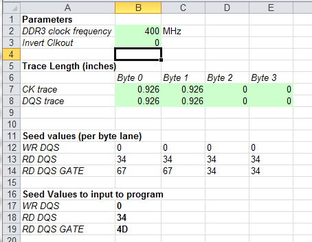
So, I tried to get the correct ratio values for the DDR3 PHY configuration. And then another issue occurs. Unlike our previous board where the CK and DQS trace lengths are about 3.5 to 4 inches long, this new board only uses 0.926 inches on both CK and DQS. Byte-wise SW leveling gave a result of 0 on all the parameters. Word-wise SW leveling gives a bunch of errors regarding RD DQS/RD DQS GATE/WR DATA RATIO MINIMUM VALUE DIDN’T CONVERGE and then gave a result of 0 on all the parameters.


Thus, a new set of questions came up.


  1. What values should be entered for Byte 2 and 3 if only 16-bit data bus width is used? We entered zero in our case.


  1. Does both DDR3 byte-wise and word-wise software leveling requires that 4-byte lane is used? Does the DDR3_SlaveRatio_ByteWiseSearch_TI814x.out and DDR_slave_ratio_search_TI814x.out know when only 2-byte lanes are used instead of 4-byte lanes?


  1. If the CK and DQS trace have equal length, what should the value of Invert Clkout be? Is it 0 or 1?


  1. What does it mean when Software Leveling is giving a result of 0 on all the required parameters? What does the error RD DQS/RD DQS GATE/WR DATA RATIO MINIMUM VALUE DIDN’T CONVERGE means?


  1. Is there a minimum DDR3 CK and DQS trace length for AM3874?


Anyway, since 0 does not seem to be an appropriate value for the DDR3 PHY configuration, I ended up using the values we were using for our previous board (even though the trace is 4 inches compared to less than 1 inch). A funny thing happened after making this change. The error in start_armboot() where gd address is incorrect was suddenly fixed. Thus, u-boot goes further. However, it will still do a data abort at a later place. U-Boot serial console message is still not present. Thus, it looks like the issue is a DDR3 configuration issue.


Any help is greatly appreciated.


Regards,
Maynard

  • Maynard,

    Maynard Cabiente said:
    Both boards are using U-Boot version based on EZSDK 5.05.02.0.

    Note that latest version of EZSDK that is tested on AM387x device is EZSDK 5.04.00.11, so could you check with the u-boot from that EZSDK.

    LINUXEZSDK-AM389X-AM387X:
    Linux EZ SDK for AM3871, AM3872, AM3874, AM3894, AM3892 - ALPHA

    Maynard Cabiente said:
    CPU is configured for 720MHz and DDR3 runs at 400MHz

    Can you try with lower DDR3 frequency?

    Maynard Cabiente said:
    Will boot from NOR flash

    Can you try with UART boot. In UART boot, the 1st stage bootloader (u-boot.min.uart) loads and run from OCMC RAM (no DDR3 involved).

    Maynard Cabiente said:

    -          Using 1 x Micron MT41K256M16HA-125 DDR3 chip (16-bit data interface, 512MB size) connected to EMIF0

    -          EMIF0 is configured for 16-bit data bus width (D0 – D15).

    -          EMIF1 is not used

    Are you aligned with the below u-boot patch?

    See also the below e2e threads regarding 16-bit DDR3 chips:

    Regards,
    Pavel

  • Hi Pavel,

    EZSDK 5.04.00.11 does not help either.

    Pavel wrote:
    > Can you try with lower DDR3 frequency?

    I tried 200MHz DDR3 with OPP100 and 333MHz with OPP100 and OPP120. None of them works. All of them encounters the data abort exception.

    Pavel wrote:
    > Can you try with UART boot. In UART boot, the 1st stage bootloader (u-boot.min.uart) loads and run from OCMC RAM (no DDR3 involved).

    Our u-boot is not setup for this at all. So, I will need some time to configure it for this.

    Pavel wrote:
    > Are you aligned with the below u-boot patch?
    > TI814x-DDR3-Init-U-Boot - Texas Instruments Wiki

    Yes. That patch was implemented since our first AM3874 custom board.

    Pavel wrote:
    > See also the below e2e threads regarding 16-bit DDR3 chips:

    Unfortunately, none of these threads help us at all. Also, all of the threads that uses x16 DDR3 uses 32-bit data bus width. Ours is different. We are just using 1 x16 DDR3 chip as a 16-bit data bus width.

    It is possible that the issue may just be DDR3 configuration. But, so far, I can't find the correct setting on 200MHz, 333MHz, or 400MHz DDR3 to make it boot-up.

    It would really be helpful to get answers to the following questions I posted before as changing the values for the DDR Software Leveling makes some difference. But, we can't use either the Byte-wise or Word-wise SW leveling because it always give us values of zeroes.

    1. What values should be entered in the TI Ratio Seed for Byte 2 and 3 if only 16-bit data bus width is used? We entered zero in our case.
    2. Does both DDR3 byte-wise and word-wise software leveling requires that 4-byte lane is used? Does the DDR3_SlaveRatio_ByteWiseSearch_TI814x.out and DDR_slave_ratio_search_TI814x.out know when only 2-byte lanes are used instead of 4-byte lanes?
    3. If the CK and DQS trace have equal length, what should the value of Invert Clkout be? Is it 0 or 1?
    4. What does it mean when Software Leveling is giving a result of 0 on all the required parameters? What does the error RD DQS/RD DQS GATE/WR DATA RATIO MINIMUM VALUE DIDN’T CONVERGE means?
    5. Is there a minimum DDR3 CK and DQS trace length for AM3874?

    Thanks,
    Maynard
  • Maynard,


    Maynard Cabiente said:
    Using 1 x Micron MT41K256M16HA-125 DDR3 chip

    See the below links where the same chip is used:

    Maynard Cabiente said:
    DDR3 has been quickly tested using Code Composer.

    Can you also run the DM814x/AM387x HW diagnostic test CCS_Code_BB/src/CCS_Test_code/Base_Board/DDR3

    This CCS test application validates the DDR memory for its ability to perform write access; read access and data storing ability. The test application writes
    a known pattern into the entire memory and then reads back the same. The known pattern written into the memory is the incremental hexadecimal numbers. After  
    writing to the entire memory area, this application reads them back and validates the data read. If the data read does not match the expected pattern, this test
    is declared failed. It is declared pass otherwise.

    BR
    Pavel

  • Hi Pavel,

    Can you please point me to where I can get the HW diagnostics test CCS_Code_BB/src/CCS_Test_code/Base_Board/DDR3? Thanks.

    Our original board was actually based on AM3352 and was using the same 1 x Micron MT41K256M16HA-125 DDR3 chip. Unfortunately, AM3352 did not meet our expectations as a result we switched to the AM3874 CPU again. We had no problem with the DDR3 chip on the AM3352. We did not have a chance to run the Software Leveling on the AM3352.

    When we tried the Software Leveling for the AM3874, that's when I encountered that the SW Leveling does not like what we input four our CK and DQS trace length and maybe the fact that we are only using 16-bit data bus width.

    Regards,
    Maynard

  • Maynard,

    Maynard Cabiente said:
    Can you please point me to where I can get the HW diagnostics test CCS_Code_BB/src/CCS_Test_code/Base_Board/DDR3?

    SOFTWARE -> Diagnostic Software -> Base Board -> rev D

    This HW diagnostic test is for the DM814x/AM387x TI EVM (see link below) so you might need to adjust it for your specific board.

    Important Note: SW leveling process is not intended to diagnose a non-working DDR interface. It is only intended for fine tuning the DDR PHY when the DDR interface is functionally working.

    It is meaningless to proceed further with SW leveling if the memory access is not working.

    See also if the below wiki pages will be in help:

    http://processors.wiki.ti.com/index.php/DM814x_Hardware_Design_Guide

    Best regards,
    Pavel

  • Maynard,

    Can you also check if your u-boot hang/stuck at the config_ti814x_ddr() function in file u-boot/board/ti/ti8148/evm.c?

    http://processors.wiki.ti.com/index.php/Understanding_u-boot-min_startup_for_DM814x

    board/ti/ti8148/evm.c

    Contains s_init() function which sets up PLLs, DDR (only when running from SRAM), and pin muxing


    /*
    * early system init of muxing and clocks.
    */
    void s_init(u32 in_ddr)
    {
    .................
    #if defined(CONFIG_TI814X_CONFIG_DDR)
    if (!in_ddr)
    config_ti814x_ddr(); /* Do DDR settings */
    #endif
    }
  • Hi Pavel,

    I found out the root cause of the 2nd data abort issue that was encountered in board_init() function. We moved the NOR_ENABLE pin (enable pin for NOR high addresses) to GPIO_0[9], which is being configured in lowlevel_init() function. In board_init(), I was configuring GPIOs already including banks 1/2/3. But, I forgot to enable the clock for these GPIO banks through CM_ALWON_GPIO_1_CLKCTRL register. Thus, when accessing GPIO1_OE or GPIOO1_SETDATAOUT registers, it will do a data abort.

    Thus, there were actually 2 different data aborts that I encountered.
    1. Data abort caused by wrong DDR PHY configuration (SW Leveling)
    2. Data abort caused by accessing disabled GPIO (i.e. GPIO clock has not been enabled)

    By fixing the second issue, I can now get u-boot serial console messages. I was able to run the memory test and it seems ok right now even though my DDR PHY configuration is probably way off. Remember that I am using values based on our other AM3874 board that has trace lengths of 3.5 to 4 inches long compared to this new board which is only 0.926 inches.

    Thus, the real concern I am focusing now is the first data abort. If I put in the wrong DDR PHY configuration based on the DDR Software Leveling, the original data abort that I encountered will pop-up back again. I re-tested this by re-using the DM8148 EVM values in our board and again it failed to boot due to data abort.

    Can you please help me out trying to get the DDR Software Leveling to run correctly on our board? Should I be using byte-wise or word-wise leveling for our board?

    Here are my original questions again.

    1. What values should be entered in the TI Ratio Seed for Byte 2 and 3 if only 16-bit data bus width is used? We entered zero in our case. Should this be left blank instead?
    2. Does both DDR3 byte-wise and word-wise software leveling requires that 4-byte lane is used? Does the DDR3_SlaveRatio_ByteWiseSearch_TI814x.out and DDR_slave_ratio_search_TI814x.out know when only 2-byte lanes are used instead of 4-byte lanes?
    3. If the CK and DQS trace have equal length, what should the value of Invert Clkout be? Is it 0 or 1?
    4. What does it mean when Software Leveling is giving a result of 0 on all the required parameters? What does the error RD DQS/RD DQS GATE/WR DATA RATIO MINIMUM VALUE DIDN’T CONVERGE means?

    Here is an example case where byte-wise SW leveling have issues. This is using the Ratio values in my original post (400 MHz DDR3).

    Enter 0 for DDR Controller 0 & 1 for DDR Controller 1
    0
    DDR START ADDR=0x80000000

    Enter the Seed Read DQS Gate Ratio Value in Hex to search the RD DQS Gate Window
    0x4d

    Enter the Seed Read DQS Ratio Value in Hex to search the RD DQS Ratio Window
    0x34

    Enter the Seed Write DQS Ratio Value in Hex to search the Write DQS Ratio Window
    0
    Enter the input file Name
    sx2_400mhz.txt

    RD DQS RATIO MINIMUM VALUE DIDN'T CONVERGE
    RD DQS RATIO MINIMUM VALUE DIDN'T CONVERGE
    RD DQS RATIO MINIMUM VALUE DIDN'T CONVERGE
    RD DQS RATIO MINIMUM VALUE DIDN'T CONVERGE
    RD DQS RATIO MINIMUM VALUE DIDN'T CONVERGE
    RD DQS RATIO MINIMUM VALUE DIDN'T CONVERGE
    RD DQS RATIO MINIMUM VALUE DIDN'T CONVERGE
    RD DQS RATIO MINIMUM VALUE DIDN'T CONVERGE
    RD DQS GATE RATIO MINIMUM VALUE DIDN'T CONVERGE
    RD DQS GATE RATIO MINIMUM VALUE DIDN'T CONVERGE
    RD DQS GATE RATIO MINIMUM VALUE DIDN'T CONVERGE
    RD DQS GATE RATIO MINIMUM VALUE DIDN'T CONVERGE
    RD DQS RATIO MINIMUM VALUE DIDN'T CONVERGE
    RD DQS RATIO MINIMUM VALUE DIDN'T CONVERGE
    RD DQS RATIO MINIMUM VALUE DIDN'T CONVERGE
    RD DQS RATIO MINIMUM VALUE DIDN'T CONVERGE
    RD DQS RATIO MINIMUM VALUE DIDN'T CONVERGE
    RD DQS RATIO MINIMUM VALUE DIDN'T CONVERGE
    RD DQS RATIO MINIMUM VALUE DIDN'T CONVERGE
    RD DQS RATIO MINIMUM VALUE DIDN'T CONVERGE
    RD DQS GATE RATIO MINIMUM VALUE DIDN'T CONVERGE
    RD DQS GATE RATIO MINIMUM VALUE DIDN'T CONVERGE
    RD DQS GATE RATIO MINIMUM VALUE DIDN'T CONVERGE
    RD DQS GATE RATIO MINIMUM VALUE DIDN'T CONVERGE
    WR DATA RATIO MAXIMUM VALUE DIDN'T CONVERGE
    WR DATA RATIO MINIMUM VALUE DIDN'T CONVERGE

    *********************************************************
    Byte level Slave Ratio Search Program Values
    *********************************************************
    BYTE3 BYTE2 BYTE1 BYTE0
    *********************************************************
    Read DQS MAX 35 0 0 0
    Read DQS MIN 0 0 0 0
    Read DQS OPT 1a 0 0 0
    *********************************************************
    Read DQS GATE MAX 0 0 0 0
    Read DQS GATE MIN 0 0 0 0
    Read DQS GATE OPT 0 0 0 0
    *********************************************************
    Write DQS MAX 0 0 0 0
    Write DQS MIN 0 0 0 0
    Write DQS OPT 0 0 0 0
    *********************************************************
    Write DATA MAX 0 0 0 0
    Write DATA MIN 0 0 0 0
    Write DATA OPT 0 0 0 0
    *********************************************************

    I appreciate all the time you are putting on this.

    Thanks,
    Maynard
  • Maynard,

    Maynard Cabiente said:
    1. What values should be entered in the TI Ratio Seed for Byte 2 and 3 if only 16-bit data bus width is used? We entered zero in our case. Should this be left blank instead?

    In both cases (0 and blank) it gives the same result. So you can enter 0.

    16-bit data bus is supported for the AM335x device SW leveling, so you might use it as a reference. Note that Word wise SW leveling is used for 32-bit and 16-bit DDR interfaces, while byte wise SW leveling is used for only 32-bit DDR interface. Word Leveling is only applicable for slow interfaces.

    http://e2e.ti.com/support/dsp/davinci_digital_media_processors/f/716/t/371898

    Maynard Cabiente said:
    2. Does both DDR3 byte-wise and word-wise software leveling requires that 4-byte lane is used? Does the DDR3_SlaveRatio_ByteWiseSearch_TI814x.out and DDR_slave_ratio_search_TI814x.out know when only 2-byte lanes are used instead of 4-byte lanes?

    I think yes (based on the below):

    Data macro for each byte lane is leveled independently. The Slave ratio search program will calculate optimal values for each byte lane.

    But this is valid for the byte wise SW leveling. It seems to me that Word wise SW leveling needs all 4 bytes, thus do not support 2 bytes only:

    The Slave ratio search program will calculate common optimal value that works for all four byte lanes.

    Maynard Cabiente said:
    3. If the CK and DQS trace have equal length, what should the value of Invert Clkout be? Is it 0 or 1?

    I think 1 (based on the below info)

    If the clock trace is longer than the DQS trace use a '0' – otherwise use a '1'

    Maynard Cabiente said:
    4. What does it mean when Software Leveling is giving a result of 0 on all the required parameters? What does the error RD DQS/RD DQS GATE/WR DATA RATIO MINIMUM VALUE DIDN’T CONVERGE means?


    See if the below link will be in help:


    BR
    Pavel

  • Hi Pavel,

    Thanks for answering the questions I have.

    Pavel Botev wrote:
    > 16-bit data bus is supported for the AM335x device SW leveling, so you might use it as a reference. Note that Word wise SW leveling is used for 32-bit and 16-bit DDR interfaces, while byte wise SW leveling is used for only 32-bit DDR interface. Word Leveling is only applicable for slow interfaces.
    >
    > Data macro for each byte lane is leveled independently. The Slave ratio search program will calculate optimal values for each byte lane.
    >
    > But this is valid for the byte wise SW leveling. It seems to me that Word wise SW leveling needs all 4 bytes, thus do not support 2 bytes only:
    >

    This is actually confusing. It is still not clear which one should be used on our 16-bit only data bus width DDR3 board: Byte-wise or Word-wise? Our intended frequency is 1 GHz AM3874 and 533 MHz DDR3. So, DDR is not a slow interface. Based on this, do I use byte-wise then?

    Pave Botev wrote:
    > If the clock trace is longer than the DQS trace use a '0' – otherwise use a '1'

    I will try this again. I did try this before and using 1 for invert clock still gives me the not converging errors and results of mostly zero on byte-wise SW leveling.

    I still need to look into all the posts you mentioned.

    But, I do have a question. On the .gel files that are provided in both byte-wise and word-wise software leveling, are we supposed to modify the values provided inside the .gel files based on our board? I do see the following definitions inside TI814x_ddr3.gel.

    //DDR3 400 MHz - CL=6,CWL=5
    #define DDR3_EMIF_TIM1_DEFINE_400 0x0AAAD4DB
    #define DDR3_EMIF_TIM2_DEFINE_400 0x682F7FDA
    #define DDR3_EMIF_TIM3_DEFINE_400 0x501F82BF
    #define DDR3_EMIF_REF_CTRL_DEFINE2_400 0x00000C30
    #define DDR3_EMIF_SDRAM_CONFIG_DEFINE_400 0x61C011B2
    #define DDR3_EMIF_DDRPHYCR_DEFINE_400 0x00170209

    //DDR3 533 MHz - CL=8,CWL=6
    #define DDR3_EMIF_TIM1_DEFINE_533 0x0EEF2664
    #define DDR3_EMIF_TIM2_DEFINE_533 0x303F7FE2
    #define DDR3_EMIF_TIM3_DEFINE_533 0x501F83AF
    #define DDR3_EMIF_REF_CTRL_DEFINE2_533 0x0000103D
    #define DDR3_EMIF_SDRAM_CONFIG_DEFINE_533 0x61C121B2
    #define DDR3_EMIF_DDRPHYCR_DEFINE_533 0x0017020B

    In our case, DDR3_EMIF_SDRAM_CONFIG should be configured for 16-bit. The default gel file assumes the board has 32-bit data bus width. Also, the TIM1, TIM2 and TIM3 settings are different for our board based on the spreadsheet on this site:

    http://processors.wiki.ti.com/index.php/File:DM814x_DDR_Controller_Register_Configuration_spreadsheet_v1.0.zip

    I also see a LISA mapping that is not meant for our board:

    /*Program the DMM to Access EMIF0 and EMIF1*/
    WR_MEM_32(DMM_LISA_MAP__0, 0x80600100);
    WR_MEM_32(DMM_LISA_MAP__1, 0x80600100);
    WR_MEM_32(DMM_LISA_MAP__2, 0xC0600200);
    WR_MEM_32(DMM_LISA_MAP__3, 0xC0600200);

    while(RD_MEM_32(DMM_LISA_MAP__0)!=0x80600100);
    while(RD_MEM_32(DMM_LISA_MAP__1)!=0x80600100);
    while(RD_MEM_32(DMM_LISA_MAP__2)!=0xC0600200);
    while(RD_MEM_32(DMM_LISA_MAP__3)!=0xC0600200);

    It is not mentioned in the TI DDR SW Leveling wiki page regarding modifying the contents of the .gel file. Should I really be changing those register values based on our board and running the byte-wise SW leveling then?

    Regards,
    Maynard
  • Maynard,

    Maynard Cabiente said:
    This is actually confusing. It is still not clear which one should be used on our 16-bit only data bus width DDR3 board: Byte-wise or Word-wise? Our intended frequency is 1 GHz AM3874 and 533 MHz DDR3. So, DDR is not a slow interface. Based on this, do I use byte-wise then?

    For 533MHz DDR3 (which is not slow), you should use byte-wise leveling. But for 16-bit DDR3 interface you should use word wise leveling. Seems to me that you can not use 533MHz with 16-bit DDR3 interface. I will double check this with our DDR3 experts and come back to you with their opinion.

    Maynard Cabiente said:
    But, I do have a question. On the .gel files that are provided in both byte-wise and word-wise software leveling, are we supposed to modify the values provided inside the .gel files based on our board?

    Maynard Cabiente said:
    It is not mentioned in the TI DDR SW Leveling wiki page regarding modifying the contents of the .gel file. Should I really be changing those register values based on our board and running the byte-wise SW leveling then?

    Yes, I think you should adjust this GEL file according to your specific board, as by default it is set to DM814x TI EVM. See also the below e2e threads which discuss the same:

    BR
    Pavel

  • Hi Pavel,

    Yes, please let me know if 533MHz is supported for 16-bit data bus width and the correct SW leveling (byte-wise or word-wise) to use once you get to discuss it with the DDR3 experts.

    Thanks,
    Maynard
  • Maynard,

    The feedback is that byte-wise leveling should be used.

    BR
    Pavel
  • Hi Pavel,

    We are still struggling with our DDR3 byte-wise software leveling. We are still in the process of getting our hardware layout verified.

    In the meantime, I do have a simple question that hopefully you would know the answer.

    As I mentioned before, we are using the AM3874 CPU. The maximum DDR data rate for this CPU is 1066. Our DDR3 chip has a speed grade of -125 (part number MT41K256M16HA-125), which is 1600 data rate.

    Which maximum data rate timing should we use for AM3874 and plug-in to the DDR_Timing_Controller_Register_Configuration_spreadsheet.xlsx? Are we limited to 1066 data rate timing only or can we use 1333 or 1600 data rate as well? Will we have issue if we actually use the 1600 data rate timing?

    Regards,
    Maynard
  • Maynard,

    Maynard Cabiente said:
    As I mentioned before, we are using the AM3874 CPU. The maximum DDR data rate for this CPU is 1066.

    See section 8.13.4.2.4.1 Compatible JEDEC DDR3 Devices

    DDR3 devices with speed grades up to DDR3-1600 are supported; however, max clock rate will still be limited to 533 MHz (same as DDR3-1066). This means you can use DDR3-1600 chips but configured for 1066 data rate (533 MHz clock rate).

    See also the below e2e thread:

    http://e2e.ti.com/support/dsp/davinci_digital_media_processors/f/716/t/271945

    BR
    Pavel

  • Hi Pavel,

    I did read the AM3874 datasheet but it was not clearly specified that user cannot use data rate timing more than 1066. Thanks for clarifying it.

    In any case, 1066 timing is what we are using in our new board. I was hoping that using 1333 or 1600 data rate timing may change the result on the byte-wise software leveling. Oh well.

    Regards,
    Maynard