This thread has been locked.

If you have a related question, please click the "Ask a related question" button in the top right corner. The newly created question will be automatically linked to this question.

66AK2H12 SRIO external termination

Other Parts Discussed in Thread: 66AK2H12

Hi,

I think that serdes interface as SRIO require the AC-coupling capacitor and external termination.
However, SRIO UG(SPRUGW1B) of 66AK2H12  described as follows:

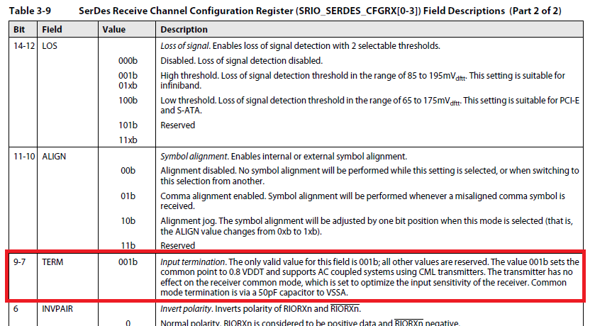
So, does this device not need external terminations because it is contain internal termination resistors?

Best regards,
H.U

  • Hi,

    I check with my hardware team and get back to you.

    Thanks,
  • Hello H.U,

    Yes, the SRIO differential TX and RX buffers contain on-chip termination resistors. The only off-chip component requirement is for DC blocking capacitors.

    Regards,

    Senthil

  • from the SERDES User's Guide (spruho3):

    All SerDes-based interfaces must be AC-coupled. As long as the SerDes link partner
    uses CML logic, the AC-coupling capacitor is the only external termination required.
    For AC-coupling, the recommendation is to use an 0402 or smaller 0.1-μF ceramic
    capacitor placed closest to the receiver BGA for all SerDes interfaces except PCIe.

    Kind regards,
    one and zero
  • Hi,

    Thank you for your reply.

    Does SRIO differential signals of 66AK2H12 not need external termination resistors when SRIO link partner use CML logic?
    In other words, if SRIO link partner use not CML logic, does SRIO differential signals of 66AK2H12 require external termination resistors?


    Best regards,
    H.U

  • Hello H.U,

    The SRIO Tx/Rx buffers has on chip termination resistors, so the external termination resistor is not needed irrespective of the link partner logic.

    Regards,
    Senthil
  • Hi, Senthil

    Thank you very much.
    I understood about on chip termination resistors.

    Best regards,
    H.U
  • Hi,

    I have additional questions.

    My customer is using only AC coupling capacitors to connect the Serdes I/F as SRIO, SGMII and PCIe.
    However, they were measured at the receive pin(SGMII_RXP/N) of 66AK2H12, The measured waveform is swinging around 0V.

    We think that the above results do not meet the DC level of the SGMII specification.

    ・Serial-GMII Specification

    Q1: Do we need DC offset with external termination?

    Q2: SRIO, PCIe is also swing to 0V center, do we should be similarly DC offset?


    Best regards,
    H.U

  • Hello H.U,

    I guess the customer is probing the signal across P and N lines. If so, the waveform would swing around 0V only as they are probing differential signal.

    The Vi in receiver DC specification shows the signal range for single ended line, either a or b. So i would suggest the customer to probe either a or b with respect to ground point and check the signal range against this specification.

    Regards,

    Senthil

  • Hi, Senthil

    Thank you for your reply.

    They are probing the signal across P and GND, N and GND. Not across P and N lines.
    In addition, Similar waveform is measured even 66AK2H12 EVM.

    We will be able to share the measurement waveform.
    However, I can not publish in E2E for confidentiality information of the customer.
    So, Would you mind if I send their summary via our local TI FAE?

    Best reards,
    H.U

  • Hello H.U,

    Yes, you could share the waveform through your local FAE.

    Regards,
    Senthil
  • Hello H.U,

    I would like to see the differential waveform also. Along with single ended waveform, please share the differential waveform as well.

    Regards,
    Senthil
  • Hi, Senthil

    I am requesting to measure the differential waveform to the customer.
    I'll tell you if i can get the waveform.

    Best regards,
    H.U
  • Hello Senthil,

    I'm Takayuki Miyazaki, Local FAE in Japan Area. Although I was looking for your e-mail address on "Directory Services", I could not reach you..

    If possible, can I have your email internally ?  you will be able to find my e-mail address on "Directory Services".

    Thank you for your patience.

    Best regards, Miyazaki

  • Hello H.U,

    The SERDES receivers all supply DC-biasing at the receivers. Series DC-blocking caps are required on these links to allow the receiver to bias the inputs as needed. The customer should connect 2 EVMs together using SRIO and then verify the signal levels in a working link. Then they can compare a functional EVM-to-EVM link to their own design.

    Regards,
    Senthil
  • Hi, Senthil

    I don't have two K2H EVMs. So, i can not try SRIO test to immediately.

    Now we are focused on Ethernet I/F(SGMII).
    SGMII_RXP/RXN are connected to ethernet PHY, so I think that we can measure whether it is biased even single EVM.


    I think that SGMII_SERDES_CGFRX0.TERM configuration is affected to bias the SGMII_RXP/RXN terminal.
    I tried the effect of this configuration with C6657EVM, because I can't found SGMII_SERDES_CGFRX0 register address in 66AK2H12 documents.
    The document(SPRUGV9D) is described that TERM field is always write 100b.
    If written 100b in this field, signals are not DC offset.
    but it seems that signals are DC offset if 000b is written

    Could you tell me the role of the TERM field and SGMII_SERDES_CGFRX0 register address of 66AK2H12?

    Best regards,
    H.U

  • Hello H.U,

    Could you tell me the role of the TERM field and SGMII_SERDES_CGFRX0 register address of 66AK2H12?

    I am not sure about the significance of TERM field in SGMII_SERDES_CGFRXn register. It should set the receiver end termination for DC biasing. I will check with the team and confirm you.

    Regarding the register address, there is a documentation issue in K2H data manual. You could refer EVMK2H technical reference manual for the configuration register address. Please refer below thread for more details.

    https://e2e.ti.com/support/dsp/c6000_multi-core_dsps/f/639/p/366562/1288994

    Regards,

    Senthil

  • Hello H.U,

    I have something to update you on TERM field.

    The SGMII_SERDES_CFGRXn register has TERM[9:7] field does set the termination for the receiver but you are incorrect in your expectation that a DC bias should be applied at the receiver.

    SGMII connections require the DC blocking capacitors between the transmitter and the receiver. For this type of connection the TERM setting of 100 is used to specify a termination with the common point around ground.

    The PHY used for SGMII is general purpose and does include capabilities for other types of termination but none of these have been tested with the KeyStone products and are not supported for use. The only setting tested is the 100 specified in SPRUGV9D. By setting these bits to 000 you have added a DC bias at the receiver which is not supported. 

    Regards,

    Senthil

  • Hi, Senthil,

    Are you say that SGMII signals to swing around grand at the Keystone products as we were measured?
    Does Keystone has input buffer which differential common mode is GND?
    So, is it not problem that does not meet the specification of SGMII?

    Best regards,
    H.U

  • Hi, Senthil,

    Please let us know the current status regarding my questions.
    We need your support.

    Best regards,
    H.U

  • Hello H.U,

    I am working with our internal team to get this answered. Thanks for your patience until then.

    Regards,
    Senthil
  • Hello, Senthil,

    Thank you for your quick reply.
    I am looking forward to your answer.

    Best regards,
    H.U
  • Hi, Senthil,

    I'm sorry to be pressing, but I am still expecting your response.

    Best regards,

    H.U

  • Hello H.U,

    Sorry for the delay. Here is the response from the internal team.

    In an AC-coupled link, the AC-coupling capacitor blocks the transmitter DC common mode voltage, so the common mode voltage is set entirely by the RX side through the TERM setting.

    For TERM setting of b’100, this requires a 0V common mode with common mode termination direct to GND.

    For TERM setting of b’000, this is for a DC-coupled link using CML transmitters with the common mode voltage determined by both the transmitter and receiver. But DC-couple link is not supported by the SGMII spec.

    Regards,
    Senthil
  • Hello, Senthil

    Thank you for your response.
    I understood that you are testing (and/or supported) at 0V common mode voltage for SGMII RX side, so SGMII signals to swing at GND is not problem.
    Is my understanding correct?


    Please forgive the additional questions.

    Q1: SRIO document is described that TERM setting is b'100 for common point to 0.8VDDT.
    Is it correct to swing around 0.8VDDT? but, SRIO signals to swing around ground when we were measured...

    Q2: Which document has been described TERM setting for PCIe?


    Best regards,
    H.U
  • Hello H.U,

    Yes, your understanding is correct.

    A1. Are you testing this using two EVM's as i mentioned in the earlier post ?

    A2. I will check on this and update you.

    Regards,
    Senthil
  • Hi, Senthil

    Thank you for your reply.

    SenthilKumar Srinivasan said:


    A1. Are you testing this using two EVM's as i mentioned in the earlier post ?

    Sorry, I have not tried yet using two EVM's.
    but, SRIO that our customer board is connected 66AK2H12 to FPGA using AC coupling, then measured Rx pin side at 66AK2H12.
    so, we think that we are considered to be the same result of our case if also it is measured using the two EVM's, because both cases are DC-blocking.
    Would the results be different  whether using EVM and FPGA, or  two EVM's?

    Best regards,
    H.U

  • Hi, Senthil

    Thank you for your reply.

    SenthilKumar Srinivasan said:

     
    A1. Are you testing this using two EVM's as i mentioned in the earlier post ?

    Sorry, I have not tried yet using two EVM's.
    but, SRIO that our customer board is connected 66AK2H12 to FPGA using AC coupling, then measured Rx pin side at 66AK2H12.
    so, we think that we are considered to be the same result of our case if also it is measured using the two EVM's, because both cases are DC-blocking.
    Would the results be different  whether using EVM and FPGA, or  two EVM's?

    Best regards,
    H.U

  • Hi, Senthil

    I'm sorry, I know you must be busy.
    Can you tell me about the progress on these question?

    Best regards,
    H.U

  • Hello H.U,

    I have requested the factory team to look into this query. Hope they will get back soon with a response.

    Thanks for your patience until then.

    Regards,
    Senthil
  • Hi, Senthil

    Any update on this issue?
    I’m sorry to be pressing, but my customer can not do their board design fix without your reply. 

    Best regards,
    H.U

  • Hi H.U,

    There appears to be some confusion on this thread. The  SGMII_SERDES_CFGRXn register which includes the TERM bits is specific to KeyStone I and does not appear in the memory map for the K2H products. The termination in the KeyStone II SOCs is not programmable and the DC common mode voltage is set to ground.  We will update the SGMII user's guide to clarify that those serdes configuration registers are specific to the KeyStone I family of components. 

    Regards,

    Bill

  • Hi, Bill

    Thank you for your reply.
    I understood that the SGMII Rx side DC common mode vlotage is set to ground for K2H product.

    but now, we are focusing about SRIO and PCIe common mode voltage,
    Please answer the following questions.

    Q1: SRIO document is described that TERM setting is b'001 for common point to 0.8VDDT.
    Is it correct to swing around 0.8VDDT? but, SRIO signals to swing around ground when we were measured...

    Q2: Which document has been described TERM setting for PCIe?

    Best regards,
    H.U

  • Hi H.U,

    I was not clear. For all KeyStone II SOCs, there is not TERM setting available for any of the serdes interfaces. The register that includes the TERM bits is only present in the KeyStone I SOCs. All KeyStone II SOCs have the DC common mode voltage set to ground for the Rx inputs. This cannot be adjusted.

    Regards,

    Bill

  • Hi, Bill

    I am grateful for your quick support.
    The reason that serdes single-end measurement is swinging around 0V at Rx input became clear.
    I expect that the document will be as soon as possible maintenance.

    Best regards,
    H.U