This thread has been locked.

If you have a related question, please click the "Ask a related question" button in the top right corner. The newly created question will be automatically linked to this question.

[C6657EVM, uPP] DLB not working...

Hi,

I'm just trying to use uPP DLB on C6657 EVM.
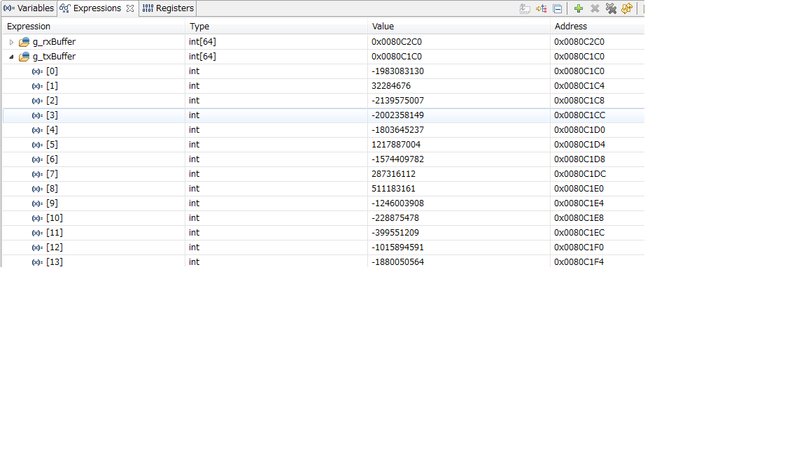
I briefly created the code to transfer data from g_txBuffer to g_rxBuffer with uPP DLB mode.
Please note I'm using CSL (C:\ti\pdk_C6657_1_1_2_6\packages\ti\csl) to build the code.

#include <ti/csl/csl_chip.h>
#include <ti/csl/csl_psc.h>
#include <ti/csl/csl_pscAux.h>
#include <ti/csl/cslr_bootcfg.h>
#include <ti/csl/cslr_upp.h>

#define REG_UPP_BASE 0x02580000
#define REG_DEVCTRL_BASE 0x02620000

#define PACKET_SIZE 64

#pragma DATA_SECTION (g_txBuffer, ".upp_buffer");
#pragma DATA_ALIGN (g_txBuffer, 64);
Int g_txBuffer[PACKET_SIZE];

#pragma DATA_SECTION (g_rxBuffer, ".upp_buffer");
#pragma DATA_ALIGN (g_rxBuffer, 64);
Int g_rxBuffer[PACKET_SIZE];

static UInt l2_global_address (UInt addr)
{
	UInt corenum;

	/* Get the core number. */
	corenum = CSL_chipReadReg(CSL_CHIP_DNUM);

	/* Compute the global address. */
	return (addr + (0x10000000 + (corenum*0x1000000)));
}

Void taskFxn(UArg a0, UArg a1)
{
    Int i;

    CSL_UppRegs *uppRegs = (CSL_UppRegs *)REG_UPP_BASE;
    CSL_BootcfgRegs *bootRegs = (CSL_BootcfgRegs *)REG_DEVCTRL_BASE;

    // Initialize rx/tx buffer
    for (i = 0; i < PACKET_SIZE; i++) {
    	g_txBuffer[i] = i;
    	g_rxBuffer[i] = 0xFFFFFFFF;
    }

    // 1 Apply the appropriate pin multiplexing settings. See the device-specific data manual, and/or
    //pin multiplexing utility for more information.

    bootRegs->CHIP_PIN_CONTROL_1 = CSL_BOOTCFG_CHIP_PIN_CONTROL_1_UPP_EMIF16_MASK;

    // 2 Enable the power and clocks to the uPP peripheral. See the device-specific data manual for more
    //information.

    //...Nothing...

    // 3 Set the SWRST bit in the uPP peripheral control register (UPPCR) to 1 to place uPP in software
    //reset.
    uppRegs->UPPCR =
    		(CSL_UPP_UPPCR_SWRST_RESET << CSL_UPP_UPPCR_SWRST_SHIFT) |
    		(CSL_UPP_UPPCR_FREE_ENABLE << CSL_UPP_UPPCR_FREE_SHIFT);

    // 4 Wait at least 200 device clock cycles, then clear the SWRST bit to 0 to bring the module out of
    //reset.
    for (i = 0; i < 200; i++) {
    	asm (" nop");
    }
    uppRegs->UPPCR &= ~CSL_UPP_UPPCR_SWRST_MASK;

    // 5 Program the uPP configuration registers: UPCTL, UPICR, UPIVR, UPTCR, and UPDLB.
    uppRegs->UPCTL =
    		(CSL_UPP_UPCTL_MODE_DUPLEX0 << CSL_UPP_UPCTL_MODE_SHIFT) |	//Using Duplex mode 0
			(CSL_UPP_UPCTL_CHN_TWO << CSL_UPP_UPCTL_CHN_SHIFT) |		//2 channels - A and B
			(CSL_UPP_UPCTL_SDRTXIL_DISABLE << CSL_UPP_UPCTL_SDRTXIL_SHIFT) |
			(CSL_UPP_UPCTL_DPWA_FULL << CSL_UPP_UPCTL_DPWA_SHIFT) |
			(CSL_UPP_UPCTL_DPWB_FULL << CSL_UPP_UPCTL_DPWB_SHIFT) |
			(CSL_UPP_UPCTL_IWA_8BIT << CSL_UPP_UPCTL_IWA_SHIFT) |
			(CSL_UPP_UPCTL_IWB_8BIT << CSL_UPP_UPCTL_IWB_SHIFT) |
			(CSL_UPP_UPCTL_DRA_SINGLE << CSL_UPP_UPCTL_DRA_SHIFT) |
			(CSL_UPP_UPCTL_DRB_SINGLE << CSL_UPP_UPCTL_DRB_SHIFT) |
			(CSL_UPP_UPCTL_DDRDEMUX_DISABLE << CSL_UPP_UPCTL_DDRDEMUX_SHIFT)
			;

    uppRegs->UPICR =
    		//Transmit -- B channel
    		//START is an output signal and is always driven.
    		//ENABLE is an output signal and is always driven.
    		//WAIT is an input signal and may be disabled using the WAITx bit in UPICR.
    		//CLOCK is an output signal.

    		(15 << CSL_UPP_UPICR_CLKDIVB_SHIFT) | // very slow clocking...
    		(CSL_UPP_UPICR_WAITPOLB_NORMAL << CSL_UPP_UPICR_WAITPOLB_SHIFT) | //WAIT is active-high
//    		(CSL_UPP_UPICR_CLKINVB_INVERT << CSL_UPP_UPICR_CLKINVB_SHIFT) | //Falling edge to send data
    		(CSL_UPP_UPICR_WAITB_ENABLE << CSL_UPP_UPICR_WAITB_SHIFT) | //Using wait signal with default polality

    		//Receive -- A channel
    		//START is an input signal and may be disabled using the STARTx bit in UPICR.
    		//ENABLE is an input signal and may be disabled using the ENAx bit in UPICR.
    		//WAIT is an output signal.
    		//CLOCK is an input signal.
    		(CSL_UPP_UPICR_STARTA_ENABLE << CSL_UPP_UPICR_STARTA_SHIFT) | //Using START signal
    		(CSL_UPP_UPICR_ENAA_ENABLE << CSL_UPP_UPICR_ENAA_SHIFT) | //Using ENA signal
    		(CSL_UPP_UPICR_CLKINVA_NORMAL << CSL_UPP_UPICR_CLKINVA_SHIFT)  //Rising edge to get data
    		;

    uppRegs->UPIVR = CSL_UPP_UPIVR_VALB_RESETVAL;
    uppRegs->UPTCR = 0; // 64byte transaction to DMAs
    uppRegs->UPDLB = CSL_UPP_UPDLB_BA_ENABLE << CSL_UPP_UPDLB_BA_SHIFT; //B to A loopback

    //6 Program the uPP interrupt enable set register (UPIES) to interrupt generation for the desired
    //events. Register an interrupt service routine (ISR) if desired; otherwise, polling is required.
    uppRegs->UPIEC = (0x1F << 8) | (0x1F); // Disable all interrupts

    //7 Set the EN bit in the uPP peripheral control register (UPPCR) to 1 to turn on the uPP peripheral.
    uppRegs->UPPCR |= CSL_UPP_UPPCR_EN_ENABLE << CSL_UPP_UPPCR_EN_SHIFT;

    //Start UPP Rx Part
    uppRegs->UPID0 = l2_global_address((UInt)g_rxBuffer);
    uppRegs->UPID1 = (1 << 16) | sizeof (g_rxBuffer);
    uppRegs->UPID2 = 0;

    //Start UPP Tx Part
    uppRegs->UPQD0 = l2_global_address((UInt)g_txBuffer);
    uppRegs->UPQD1 = (1 << 16) | sizeof (g_txBuffer);
    uppRegs->UPQD2 = 0;

    while (1) {
    	asm(" nop");
    }
}

When the control reaches to "nop", I think the transfer should happen, but actually,no transfer.
Do you have any suggestions ? Please note tx/rx buffer has been allocated in L2RAM. So, I don't implement cache related code to tx/rx buffer.
What I want to check with this code is to evaluate the latency in uPP. So,I'm doing only minimal configurations to uPP. 

Please check the following link about the background.

http://e2e.ti.com/support/dsp/c6000_multi-core_dsps/f/639/t/390898

Best Regards,
Kawada

  • Hi Kawada,

    Please refer the below uPP driver wiki on OMAP-L1x platforms. Please refer the demo code to verify the uPP init are done correctly for DLB testing.

    Also refer below e2e thread,

  • Hi,

    Unfortunately, I've been getting stuck yet.

    I found one mistake in the above code. I accessed PIN_CONTROL_1 register by using CSL, but the address of bootRegs->CHIP_PIN_CONTROL_1 was incorrect, i.e., it was *not* 0x02620584 ! I believe the definition of CSL_BootcfgRegs structure is incorrect. So, I changed my code as below. Also, I've done the minimal changes about UPP configurations:

    #include <ti/csl/csl_chip.h>
    #include <ti/csl/csl_psc.h>
    #include <ti/csl/csl_pscAux.h>
    #include <ti/csl/cslr_bootcfg.h>
    #include <ti/csl/cslr_upp.h>
    
    /*
     *  ======== taskFxn ========
     */
    
    #define REG_UPP_BASE 0x02580000
    #define REG_DEVCTRL_BASE 0x02620000
    
    #define PACKET_SIZE 64
    
    #pragma DATA_SECTION (g_txBuffer, ".upp_buffer");
    #pragma DATA_ALIGN (g_txBuffer, 64);
    Int g_txBuffer[PACKET_SIZE];
    
    #pragma DATA_SECTION (g_rxBuffer, ".upp_buffer");
    #pragma DATA_ALIGN (g_rxBuffer, 64);
    Int g_rxBuffer[PACKET_SIZE];
    
    static UInt l2_global_address (UInt addr)
    {
    	UInt corenum;
    
    	/* Get the core number. */
    	corenum = CSL_chipReadReg(CSL_CHIP_DNUM);
    
    	/* Compute the global address. */
    	return (addr + (0x10000000 + (corenum*0x1000000)));
    }
    
    Void taskFxn(UArg a0, UArg a1)
    {
    	Int i;
    
        CSL_UppRegs *uppRegs = (CSL_UppRegs *)REG_UPP_BASE;
        //CSL_BootcfgRegs *bootRegs = (CSL_BootcfgRegs *)REG_DEVCTRL_BASE;
    
        // Initialize rx/tx buffer
        for (i = 0; i < PACKET_SIZE; i++) {
        	g_txBuffer[i] = i;
        	g_rxBuffer[i] = 0xFFFFFFFF;
        }
    
        // 1 Apply the appropriate pin multiplexing settings. See the device-specific data manual, and/or
        //pin multiplexing utility for more information.
    
        //bootRegs->CHIP_PIN_CONTROL_1 = CSL_BOOTCFG_CHIP_PIN_CONTROL_1_UPP_EMIF16_MASK;
        //addr = (UInt)&(bootRegs->CHIP_PIN_CONTROL_1);
    
        *(volatile UInt *)0x02620584 = 0x00000001; // PIN_CONTROL_1 regisger config -- use UPP
        *(volatile UInt *)0x0262016C = 0x00000000; // UPP_CONTROL register config -- use SYSCLK4 (CPU/3)
    
        // 2 Enable the power and clocks to the uPP peripheral. See the device-specific data manual for more
        //information.
    
        //...Nothing...
    
        // 3 Set the SWRST bit in the uPP peripheral control register (UPPCR) to 1 to place uPP in software
        //reset.
        uppRegs->UPPCR =
        		(CSL_UPP_UPPCR_SWRST_RESET << CSL_UPP_UPPCR_SWRST_SHIFT) |
        		(CSL_UPP_UPPCR_FREE_ENABLE << CSL_UPP_UPPCR_FREE_SHIFT);
    
        // 4 Wait at least 200 device clock cycles, then clear the SWRST bit to 0 to bring the module out of
        //reset.
        for (i = 0; i < 200; i++) {
        	asm (" nop");
        }
        uppRegs->UPPCR &= ~CSL_UPP_UPPCR_SWRST_MASK;
    
        // 5 Program the uPP configuration registers: UPCTL, UPICR, UPIVR, UPTCR, and UPDLB.
        uppRegs->UPCTL =
        		(CSL_UPP_UPCTL_MODE_DUPLEX0 << CSL_UPP_UPCTL_MODE_SHIFT) |	//Using Duplex mode 0
    			(CSL_UPP_UPCTL_CHN_TWO << CSL_UPP_UPCTL_CHN_SHIFT) |		//2 channels - A and B
    			(CSL_UPP_UPCTL_SDRTXIL_DISABLE << CSL_UPP_UPCTL_SDRTXIL_SHIFT) |
    			(CSL_UPP_UPCTL_DPWA_FULL << CSL_UPP_UPCTL_DPWA_SHIFT) |
    			(CSL_UPP_UPCTL_DPWB_FULL << CSL_UPP_UPCTL_DPWB_SHIFT) |
    			(CSL_UPP_UPCTL_IWA_8BIT << CSL_UPP_UPCTL_IWA_SHIFT) |
    			(CSL_UPP_UPCTL_IWB_8BIT << CSL_UPP_UPCTL_IWB_SHIFT) |
    			(CSL_UPP_UPCTL_DRA_SINGLE << CSL_UPP_UPCTL_DRA_SHIFT) |
    			(CSL_UPP_UPCTL_DRB_SINGLE << CSL_UPP_UPCTL_DRB_SHIFT) |
    			(CSL_UPP_UPCTL_DDRDEMUX_DISABLE << CSL_UPP_UPCTL_DDRDEMUX_SHIFT) |
    			(CSL_UPP_UPCTL_DPFA_RJZE << CSL_UPP_UPCTL_DPFA_SHIFT) |
    			(CSL_UPP_UPCTL_DPFB_RJZE << CSL_UPP_UPCTL_DPFB_SHIFT)
    			;
    
        uppRegs->UPICR =
        		//Transmit -- B channel
        		//START is an output signal and is always driven.
        		//ENABLE is an output signal and is always driven.
        		//WAIT is an input signal and may be disabled using the WAITx bit in UPICR.
        		//CLOCK is an output signal.
    
        		(15 << CSL_UPP_UPICR_CLKDIVB_SHIFT) | // very slow clocking...
    //    		(CSL_UPP_UPICR_CLKINVB_INVERT << CSL_UPP_UPICR_CLKINVB_SHIFT) | //Falling edge to send data
        		(CSL_UPP_UPICR_WAITB_ENABLE << CSL_UPP_UPICR_WAITB_SHIFT) | //Using wait signal with default polality
        		(CSL_UPP_UPICR_STARTB_ENABLE << CSL_UPP_UPICR_STARTB_SHIFT) | //Using START signal
        		(CSL_UPP_UPICR_ENAB_ENABLE << CSL_UPP_UPICR_ENAB_SHIFT) | //Using ENA signal
    
        		//Receive -- A channel
        		//START is an input signal and may be disabled using the STARTx bit in UPICR.
        		//ENABLE is an input signal and may be disabled using the ENAx bit in UPICR.
        		//WAIT is an output signal.
        		//CLOCK is an input signal.
        		(CSL_UPP_UPICR_STARTA_ENABLE << CSL_UPP_UPICR_STARTA_SHIFT) | //Using START signal
        		(CSL_UPP_UPICR_ENAA_ENABLE << CSL_UPP_UPICR_ENAA_SHIFT) | //Using ENA signal
        		(CSL_UPP_UPICR_CLKINVA_NORMAL << CSL_UPP_UPICR_CLKINVA_SHIFT)  //Rising edge to get data
        		;


        uppRegs->UPIVR = CSL_UPP_UPIVR_VALB_RESETVAL;
    
        uppRegs->UPTCR = 0; // 64byte transaction to DMAs
    
        uppRegs->UPDLB = CSL_UPP_UPDLB_BA_ENABLE << CSL_UPP_UPDLB_BA_SHIFT; //B to A loopback
    
        //6 Program the uPP interrupt enable set register (UPIES) to interrupt generation for the desired
        //events. Register an interrupt service routine (ISR) if desired; otherwise, polling is required.
        uppRegs->UPIES = (0x1F << 8) | (0x1F); // Enable all interrupts, but no handling for them...
    
        //7 Set the EN bit in the uPP peripheral control register (UPPCR) to 1 to turn on the uPP peripheral.
        uppRegs->UPPCR |= CSL_UPP_UPPCR_EN_ENABLE << CSL_UPP_UPPCR_EN_SHIFT;
    
        // Wait pend bit is cleared before starting rx
        while (uppRegs->UPIS2 & CSL_UPP_UPIS2_PEND_MASK);
    
        //Start UPP Rx Part
        uppRegs->UPID0 = l2_global_address((UInt)g_rxBuffer);
    
        uppRegs->UPID1 = (1 << 16) | sizeof (g_rxBuffer);
    
        uppRegs->UPID2 = 0;
    
        // Wait pend bit is cleared before starting tx
        while (uppRegs->UPQS2 & CSL_UPP_UPQS2_PEND_MASK);
    
        //Start UPP Tx Part
        uppRegs->UPQD0 = l2_global_address((UInt)g_txBuffer);
    
        uppRegs->UPQD1 = (1 << 16) | sizeof (g_txBuffer);
    
        uppRegs->UPQD2 = 0;
    
        while (1) {
        	asm(" nop");
        }
    

    With this code, uPP started to work, but its behavior is *very* strange! i.e., when the control went to "nop" in the above code, the contents of tx buffer was clashed .
    Please note g_txBuffer has been initialized correctly before starting uPP.

    Here is a snap shot. As you see, g_txBuffer is being clashed.


    At this point, UPISR (0x02580020) indicated 0x00000018 (End of line/window events detected). So this means the transfer has been completed, but something incorrect data have been routed to g_txBuffer, rather than g_rxBuffer. Also, after EVM power cycle, I inverted the polarity of CLOCK_B (uncomment the code : (CSL_UPP_UPICR_CLKINVB_INVERT << CSL_UPP_UPICR_CLKINVB_SHIFT) | //Falling edge to send data), and then this issue did not happen, but the g_txBuffer was not transferred to g_rxBuffer.

    I'm concerned if uPP is really available on this device... Can you check this issue at your end ? I believe you can recreate the issue easily.

    Best Regards,
    Kawada


  • Hi Kawada,

    The device C6657 has uPP.  Have you referred the driver and "test" from below link?

  • Hi Rajasekaran K,

    Actually, I had reviewed biospsp_01_30_01 upp driver implementation and noticed the workaround for DLB mode. Here is from Upp.c:

                        /* Note: In DLB mode both the sections require the same   *
                         * clkdiv values other wise the DLB mode does not work    *
                         * properly                                               */
                        if (Upp_Loopback_ENABLE_AB == instHandle->devParams.dlbMode)
                        {
                            /* copy the CLK div values from the channel A to B    */
                            instHandle->upicrRegVal |=
                                (((instHandle->upicrRegVal &
                                   CSL_UPP_UPICR_CLKDIVA_MASK) >>
                                   CSL_UPP_UPICR_CLKDIVA_SHIFT) <<
                                   CSL_UPP_UPICR_CLKDIVB_SHIFT);
                        }
                        else if (Upp_Loopback_ENABLE_BA
                            == instHandle->devParams.dlbMode)
                        {
                            /* copy the CLK div values from the channel B to A    */
                            instHandle->upicrRegVal |=
                                (((instHandle->upicrRegVal &
                                   CSL_UPP_UPICR_CLKDIVB_MASK) >>
                                   CSL_UPP_UPICR_CLKDIVB_SHIFT) <<
                                   CSL_UPP_UPICR_CLKDIVA_SHIFT);
                        }

    And I had tried the same in my code:

        uppRegs->UPICR =
        		//Transmit -- B channel
        		//START is an output signal and is always driven.
        		//ENABLE is an output signal and is always driven.
        		//WAIT is an input signal and may be disabled using the WAITx bit in UPICR.
        		//CLOCK is an output signal.
    
        		(15 << CSL_UPP_UPICR_CLKDIVB_SHIFT) | // very slow clocking...
    //    		(CSL_UPP_UPICR_CLKINVB_INVERT << CSL_UPP_UPICR_CLKINVB_SHIFT) | //Falling edge to send data
        		(CSL_UPP_UPICR_WAITB_ENABLE << CSL_UPP_UPICR_WAITB_SHIFT) | //Using wait signal with default polality
        		(CSL_UPP_UPICR_STARTB_ENABLE << CSL_UPP_UPICR_STARTB_SHIFT) | //Using START signal
        		(CSL_UPP_UPICR_ENAB_ENABLE << CSL_UPP_UPICR_ENAB_SHIFT) | //Using ENA signal
    
        		//Receive -- A channel
        		//START is an input signal and may be disabled using the STARTx bit in UPICR.
        		//ENABLE is an input signal and may be disabled using the ENAx bit in UPICR.
        		//WAIT is an output signal.
        		//CLOCK is an input signal.
        		(15 << CSL_UPP_UPICR_CLKDIVA_SHIFT) | // very slow clocking...(biospsp_01_30_01 is configuring both CLOCKDIVA and CLOKCDIVB when DLB mode is used)
        		(CSL_UPP_UPICR_STARTA_ENABLE << CSL_UPP_UPICR_STARTA_SHIFT) | //Using START signal
        		(CSL_UPP_UPICR_ENAA_ENABLE << CSL_UPP_UPICR_ENAA_SHIFT) | //Using ENA signal
        		(CSL_UPP_UPICR_CLKINVA_NORMAL << CSL_UPP_UPICR_CLKINVA_SHIFT)  //Rising edge to get data
        		;

    As you see, I'm using same value for both CLOCKDIVA and CLOCKDIVB (I believe we don't have to configure CLOCKDIVA because only channel B should generate CLOCK in my case, but I had tried this because biospsp is doing). 

    As a result, I can see no progress on this issue. Exactly same issue is still existing.

    Do you have any other suggestions ?
    I don't really understand why g_txBuffer is routed to g_txBuffer (with clashed data), rather than g_rxBuffer.....

    Best  Regards,
    Kawada

  • Hi Kawada,
    We will setup a test environment for this and let you know. Thank you for your patience.
  • Hi Rajasekaran K,

    Thank you very much for all your help! Ok, I'll wait for your updates. For a meanwhile, I'll keep confirming the issue at my side.

    Best Regards,
    Kawada
  • Hi Kawada,
    We tried re-producing the issue. The Tx buffer is not over written. We think, the issue may be with memory configuration(.cmd). Could you please share the complete project?
  • Hi,

    Please find the example code for upp dlb test in below thread,

    Thank you.

  • Hi Pubesh,

    Thanks for your confirmation! Ok, you don't see the problem...
    I shared my project.
    sample_c6657_upp_loopback.zip

    As you see, the g_txBuffer/g_rxBuffer are configured to allocate to L2RAM in linker.cmd : 

    SECTIONS {
    .upp_buffer :> L2SRAM
    .upp_buffer :> L2SRAM
    }

    Now I noticed .upp_buffer section is allocated doubly. Sorry this is just my typo, but I confirmed g_txBuffer and g_rxBuffer are allocated to L2SRAM with separate address. Please find *.map file. So this should not be a matter.

    0080c1c0 g_txBuffer
    0080c2c0 g_rxBuffer

    We are in year end vacation. So the response would be delayed.

    Best Regards,
    Kawada

  • Hi,

    I have just come back from my vacation.
    I checked the gel file and I noticed boot config register should be accessed via lock/unlock mechanism.
    And I just add this to my code and confirmed my code worked. I'll post the complete code here later.

    Best Regards,
    kawada

  • Hi

    Here is a complete code.

    5700.sample_c6657_upp_loopback.zip

    With this code, I verified uPP loopback on c6657 EVM.

    As I mentioned in the previous post, the problem was not uPP register configurations, but no configuration of KICK0/1 registers.
    (I don't know why I could see txbuffer-overwrite without the configurations of KICK0/1 registers, but now this is not a matter with me)

    If you run the code, you would see the following log in CCS console. That is a latency taken by DLB (256 bytes looping from L2 tx buffer to L2 rx buffer, with 4 divisor for channel B clocking. As for other conditions, please see the code)

    UPP latency : 7957 cycle


    I'm afraid that I have troubled you so much with this thread.
    Thank you very much for all your helps.

    The last input to you is that the definition of CSL_BootcfgRegs structure is wrong. For example, The address of bootRegs->CHIP_PIN_CONTROL_1 is not 0x02620584. So the fix should be taken into account in future release of CSL.

    Best Regards,
    Kawada