This thread has been locked.

If you have a related question, please click the "Ask a related question" button in the top right corner. The newly created question will be automatically linked to this question.

Power Management

Other Parts Discussed in Thread: SYSBIOS, TEST2, OMAPL138

Dear TI.

We´re working in a video application and we´re using the C6748 (without DSP-BIOS or SYS-BIOS), we almost create the final product, there are few things left. One of those things is regarding with low power. We tried over and over and now we’re stuck and we need your help. In ordered to expose the problem and accelerate the solution we present the followed step that we did:

1. We followed the C6748 Technical Reference Manual” in order to decrease the power consumption. And according with it, we change the PLL0/PLL1 configuration (bypass/ power down). It works fine because in debug mode (CCS) the current descend from 110 mA to 55 mA and the rest of the consecutive instructions were executed at slowly rate.

2. We tried to restore the PLL0/PLL1 taking the procedure described in the Reference Manual for that, but fail. The system is stuck in some place.

3. We used the Core_300MHz_mDDR_150MHz function presented in the gel file (C6748_LCDK.gel) and we could restore the PLL0/PLL1 (at 300 MHz). How did we do this? In debug operation we put a breaking point after the PLL0/PLL1 bypass/power-down. Then we call the Core_300MHz_mDDR_150MHz (in CCS ->Scripts) and voila the system recovery to the original setup.

4. So, we copied the Core_300MHz_mDDR_150MHz from the C6748_LCDK.gel into our project (with minimum adaptation), but we can´t restore the PLL0/PLL1.

5. We tried in release mode and burning the flash and the problem remains, The DSP is still stuck in some point.


In order to clarify the point number 4 described above we present Fig. 1 with our functions. When the function LowPower is call everything seems to work fine the problem is when we try to call the RestorePower function.


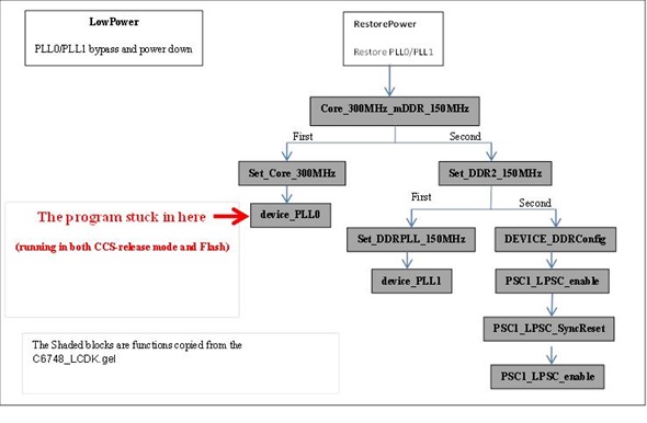
  Fig. 1. Functions for power management.


The code for LowPower and RestorePower are presented in the next paragraphs.


void LowPower()

{

                HWREG(KICK0R)=0x83E70B13;

                HWREG(KICK0R)=0x83E70B13;

                HWREG(KICK1R)=0x95A4F1E0;

                CFGCHIP0&=0xFFFFFFEF;

                CFGCHIP3&=0xFFFFFFDF;

                // Set PLLENSRC '0',bit 5, PLL Enable(PLLEN) selection is controlled through MMR

                PLL0_PLLCTL &= ~(0x00000020);

                // PLLCTL.EXTCLKSRC bit 9 should be left at 0 for Freon

                PLL0_PLLCTL &= ~(0x00000200);

                // Set PLLEN=0 to put in bypass mode

                PLL0_PLLCTL &= ~(0x00000001);

                //wait for 4 cycles to allow PLLEN mux switches properly to bypass clock

                for(int i=0; i<PLLEN_MUX_SWITCH; i++) { }

// Set PLLENSRC '0',bit 5, PLL Enable(PLLEN) selection is controlled through MMR

                PLL1_PLLCTL &= ~(0x00000020);

                // PLLCTL.EXTCLKSRC bit 9 should be left at 0 for Freon

                PLL1_PLLCTL &= ~(0x00000200);

                // Set PLLEN=0 to put in bypass mode

                PLL1_PLLCTL &= ~(0x00000001);

                //wait for 4 cycles to allow PLLEN mux switches properly to bypass clock

                for(int i=0; i<PLLEN_MUX_SWITCH; i++) { }

//PLL1 Power down

                PLL1_PLLCTL=PLL1_PLLCTL|0x2;    

//PLL0 Power down

PLL0_PLLCTL=PLL0_PLLCTL|0x2;   

}

void RestorePower()

{

HWREG(KICK0R)=0x83E70B13;

                HWREG(KICK0R)=0x83E70B13;

                HWREG(KICK1R)=0x95A4F1E0;

                CFGCHIP0&=0xFFFFFFEF;

                CFGCHIP3&=0xFFFFFFDF;

Core_300MHz_mDDR_150MHz();

}

Our full code including the Core_300MHz_mDDR_150MHz function is taken from the gel file and is presented in the bottom of this post.

Would you like to help us to PLL bypass/power down and then restore the PLL?


One more last thing, we noted a current difference when the program is running in debug mode (CCS v5.1) and when the program is running from FLASH. The difference is 30 mA more (running in Flash). This is normal? We use the AISge tool with configurations file like the follow.


Boot Mode=NAND Flash
Boot Speed=115200
Flash Width=1
Flash Timing=3ffffffd
Configure Peripheral=False
Configure PLL0=True
Configure SDRAM=False
Configure PLL1=True
Configure DDR2=True
Configure LPSC=False
Configure Pinmux=False
Enable CRC=False
Specify Entrypoint=False
Enable Sequential Read=False
Use 4.5 Clock Divider=False
Use DDR2 Direct Clock=False
Use mDDR=False
ROM ID=3
Device Type=1
Input Clock Speed=24
Clock Type=0
PLL0 Pre Divider=1
PLL0 Multiplier=25
PLL0 Post Divider=2
PLL0 Div1=1
PLL0 Div3=3
PLL0 Div7=6
PLL1 Multiplier=25
PLL1 Post Divider=2
PLL1 Div1=1
PLL1 Div2=2
PLL1 Div3=3
Entrypoint=c1080000
SDRAM SDBCR=0
SDRAM SDTMR=0
SDRAM SDRSRPDEXIT=0
SDRAM SDRCR=0
DDR2 PHY=c5
DDR2 SDCR=134832
DDR2 SDCR2=0
DDR2 SDTIMR=264a3209
DDR2 SDTIMR2=3c14c722
DDR2 SDRCR=492
LPSC0 Enable=0+1+2+3+4+5+9+11+12+
LPSC0 Disable=
LPSC0 SyncRst=
LPSC1 Enable=0+1+2+3+4+5+7+9+10+11+12+13+14+15+16+18+
LPSC1 Disable=
LPSC1 SyncRst=
Pinmux=
App File String=C:\ti\C6748_StarterWare_1_20_03_03\build\c674x\cgt_ccs\c6748\lcdkC6748\vpif_lcd_loopback\Release\vpif_lcd_loopback.out;
AIS File Name=C:\temp\vpif_lcd_loopback.bin


Thank you in advance and we hope to find the answer for this issue.


FULL CODE:

#define LPSC_EDMA_CC0 0 #define LPSC_EDMA_TC0 1 #define LPSC_EDMA_TC1 2 #define LPSC_EMIFA 3 /*PSC0*/ #define LPSC_SPI0 4 /*PSC0*/ #define LPSC_MMCSD0 5 /*PSC0*/ #define LPSC_ARM_AINTC 6 #define LPSC_ARM_RAMROM 7 /*PSC0*/ // LPSC #8 not used #define LPSC_UART0 9 /*PSC0*/ #define LPSC_SCR0 10 #define LPSC_SCR1 11 #define LPSC_SCR2 12 // LPSC #13 not used #define LPSC_ARM 14 /*PSC0*/ #define LPSC_DSP 15 /*PSC0*/ #define LPSC_EDMA_CC1 0 #define LPSC_USB20 1 /*PSC1*/ #define LPSC_USB11 2 /*PSC1*/ #define LPSC_GPIO 3 /*PSC1*/ #define LPSC_UHPI 4 /*PSC1*/ #define LPSC_EMAC 5 /*PSC1*/ #define LPSC_DDR 6 /*PSC1*/ #define LPSC_MCASP0 7 /*PSC1*/ #define LPSC_SATA 8 /*PSC1*/ #define LPSC_VPIF 9 /*PSC1*/ #define LPSC_SPI1 10 /*PSC1*/ #define LPSC_I2C1 11 /*PSC1*/ #define LPSC_UART1 12 /*PSC1*/ #define LPSC_UART2 13 /*PSC1*/ #define LPSC_MCBSP0 14 /*PSC1*/ #define LPSC_MCBSP1 15 /*PSC1*/ #define LPSC_LCDC 16 /*PSC1*/ #define LPSC_EPWM 17 /*PSC1*/ #define LPSC_MMCSD1 18 #define LPSC_UPP 19 #define LPSC_ECAP 20 #define LPSC_EDMA_TC2 21 // LPSC #22-23 not used #define LPSC_SCR_F0 24 #define LPSC_SCR_F1 25 #define LPSC_SCR_F2 26 #define LPSC_SCR_F6 27 #define LPSC_SCR_F7 28 #define LPSC_SCR_F8 29 #define LPSC_BR_F7 30 #define LPSC_SHARED_RAM 31 /*PSC Module Related Registers*/ #define PSC0_BASE 0x01C10000 #define PSC1_BASE 0x01E27000 #define PSC0_MDCTL (PSC0_BASE+0xA00) #define PSC0_MDSTAT (PSC0_BASE+0x800) #define PSC0_PTCMD *(unsigned int*) (PSC0_BASE + 0x120) #define PSC0_PTSTAT *(unsigned int*) (PSC0_BASE + 0x128) #define PSC1_MDCTL (PSC1_BASE+0xA00) #define PSC1_MDSTAT (PSC1_BASE+0x800) #define PSC1_PTCMD *(volatile unsigned int*) (PSC1_BASE + 0x120) #define PSC1_PTSTAT *(volatile unsigned int*) (PSC1_BASE + 0x128) #define PSC_TIMEOUT 200 // This value can be optimized by the user #define PLL0_BASE 0x01C11000 /*SYSTEM PLL BASE ADDRESS*/ #define PLL0_PID *(volatile unsigned int*) (PLL0_BASE + 0x00) /*PID*/ #define PLL0_RSTYPE *(volatile unsigned int*) (PLL0_BASE + 0xE4) /*Reset Type status Reg*/ #define PLL0_PLLCTL *(volatile unsigned int*) (PLL0_BASE + 0x100) /*PLL Control Register*/ #define PLL0_OCSEL *(volatile unsigned int*) (PLL0_BASE + 0x104) /*OBSCLK Select Register*/ #define PLL0_SECCTL *(volatile unsigned int*) (PLL0_BASE + 0x108) /*PLL Secondary Control Register*/ #define PLL0_PLLM *(volatile unsigned int*) (PLL0_BASE + 0x110) /*PLL Multiplier*/ #define PLL0_PREDIV *(volatile unsigned int*) (PLL0_BASE + 0x114) /*Pre divider*/ #define PLL0_PLLDIV1 *(volatile unsigned int*) (PLL0_BASE + 0x118) /*Divider-1*/ #define PLL0_PLLDIV2 *(volatile unsigned int*) (PLL0_BASE + 0x11C) /*Divider-2*/ #define PLL0_PLLDIV3 *(volatile unsigned int*) (PLL0_BASE + 0x120) /*Divider-3*/ #define PLL0_OSCDIV1 *(volatile unsigned int*) (PLL0_BASE + 0x124) /*Oscilator Divider*/ #define PLL0_POSTDIV *(volatile unsigned int*) (PLL0_BASE + 0x128) /*Post Divider*/ #define PLL0_BPDIV *(volatile unsigned int*) (PLL0_BASE + 0x12C) /*Bypass Divider*/ #define PLL0_WAKEUP *(volatile unsigned int*) (PLL0_BASE + 0x130) /*Wakeup Reg*/ #define PLL0_PLLCMD *(volatile unsigned int*) (PLL0_BASE + 0x138) /*Command Reg*/ #define PLL0_PLLSTAT *(volatile unsigned int*) (PLL0_BASE + 0x13C) /*Status Reg*/ #define PLL0_ALNCTL *(volatile unsigned int*) (PLL0_BASE + 0x140) /*Clock Align Control Reg*/ #define PLL0_DCHANGE *(volatile unsigned int*) (PLL0_BASE + 0x144) /*PLLDIV Ratio Chnage status*/ #define PLL0_CKEN *(volatile unsigned int*) (PLL0_BASE + 0x148) /*Clock Enable Reg*/ #define PLL0_CKSTAT *(volatile unsigned int*) (PLL0_BASE + 0x14C) /*Clock Status Reg*/ #define PLL0_SYSTAT *(volatile unsigned int*) (PLL0_BASE + 0x150) /*Sysclk status reg*/ #define PLL0_PLLDIV4 *(volatile unsigned int*) (PLL0_BASE + 0x160) /*Divider 4*/ #define PLL0_PLLDIV5 *(volatile unsigned int*) (PLL0_BASE + 0x164) /*Divider 5*/ #define PLL0_PLLDIV6 *(volatile unsigned int*) (PLL0_BASE + 0x168) /*Divider 6*/ #define PLL0_PLLDIV7 *(volatile unsigned int*) (PLL0_BASE + 0x16C) /*Divider 7*/ #define PLL0_PLLDIV8 *(volatile unsigned int*) (PLL0_BASE + 0x170) /*Divider 8*/ #define PLL0_PLLDIV9 *(volatile unsigned int*) (PLL0_BASE + 0x174) /*Divider 9*/ #define PLL0_PLLDIV10 *(volatile unsigned int*) (PLL0_BASE + 0x178) /*Divider 10*/ #define PLL0_PLLDIV11 *(volatile unsigned int*) (PLL0_BASE + 0x17C) /*Divider 11*/ #define PLL0_PLLDIV12 *(volatile unsigned int*) (PLL0_BASE + 0x180) /*Divider 12*/ #define PLL0_PLLDIV13 *(volatile unsigned int*) (PLL0_BASE + 0x184) /*Divider 13*/ #define PLL0_PLLDIV14 *(volatile unsigned int*) (PLL0_BASE + 0x188) /*Divider 14*/ #define PLL0_PLLDIV15 *(volatile unsigned int*) (PLL0_BASE + 0x18C) /*Divider 15*/ #define PLL0_PLLDIV16 *(volatile unsigned int*) (PLL0_BASE + 0x190) /*Divider 16*/ #define PLL1_BASE 0x01E1A000 /*SYSTEM PLL1 BASE ADDRESS*/ #define PLL1_PID *(volatile unsigned int*) (PLL1_BASE + 0x00) /*PID*/ #define PLL1_RSTYPE *(volatile unsigned int*) (PLL1_BASE + 0xE4) /*Reset Type status Reg*/ #define PLL1_PLLCTL *(volatile unsigned int*) (PLL1_BASE + 0x100) /*PLL Control Register*/ #define PLL1_OCSEL *(volatile unsigned int*) (PLL1_BASE + 0x104) /*OBSCLK Select Register*/ #define PLL1_SECCTL *(volatile unsigned int*) (PLL1_BASE + 0x108) /*PLL Secondary Control Register*/ #define PLL1_PLLM *(volatile unsigned int*) (PLL1_BASE + 0x110) /*PLL Multiplier*/ #define PLL1_PREDIV *(volatile unsigned int*) (PLL1_BASE + 0x114) /*Pre divider*/ #define PLL1_PLLDIV1 *(volatile unsigned int*) (PLL1_BASE + 0x118) /*Divider-1*/ #define PLL1_PLLDIV2 *(volatile unsigned int*) (PLL1_BASE + 0x11C) /*Divider-2*/ #define PLL1_PLLDIV3 *(volatile unsigned int*) (PLL1_BASE + 0x120) /*Divider-3*/ #define PLL1_OSCDIV1 *(volatile unsigned int*) (PLL1_BASE + 0x124) /*Oscilator Divider*/ #define PLL1_POSTDIV *(volatile unsigned int*) (PLL1_BASE + 0x128) /*Post Divider*/ #define PLL1_BPDIV *(volatile unsigned int*) (PLL1_BASE + 0x12C) /*Bypass Divider*/ #define PLL1_WAKEUP *(volatile unsigned int*) (PLL1_BASE + 0x130) /*Wakeup Reg*/ #define PLL1_PLLCMD *(volatile unsigned int*) (PLL1_BASE + 0x138) /*Command Reg*/ #define PLL1_PLLSTAT *(volatile unsigned int*) (PLL1_BASE + 0x13C) /*Status Reg*/ #define PLL1_ALNCTL *(volatile unsigned int*) (PLL1_BASE + 0x140) /*Clock Align Control Reg*/ #define PLL1_DCHANGE *(volatile unsigned int*) (PLL1_BASE + 0x144) /*PLLDIV Ratio Chnage status*/ #define PLL1_CKEN *(volatile unsigned int*) (PLL1_BASE + 0x148) /*Clock Enable Reg*/ #define PLL1_CKSTAT *(volatile unsigned int*) (PLL1_BASE + 0x14C) /*Clock Status Reg*/ #define PLL1_SYSTAT *(volatile unsigned int*) (PLL1_BASE + 0x150) /*Sysclk status reg*/ #define PLL1_PLLDIV4 *(volatile unsigned int*) (PLL1_BASE + 0x160) /*Divider 4*/ #define PLL1_PLLDIV5 *(volatile unsigned int*) (PLL1_BASE + 0x164) /*Divider 5*/ #define PLL1_PLLDIV6 *(volatile unsigned int*) (PLL1_BASE + 0x168) /*Divider 6*/ #define PLL1_PLLDIV7 *(volatile unsigned int*) (PLL1_BASE + 0x16C) /*Divider 7*/ #define PLL1_PLLDIV8 *(volatile unsigned int*) (PLL1_BASE + 0x170) /*Divider 8*/ #define PLL1_PLLDIV9 *(volatile unsigned int*) (PLL1_BASE + 0x174) /*Divider 9*/ #define PLL1_PLLDIV10 *(volatile unsigned int*) (PLL1_BASE + 0x178) /*Divider 10*/ #define PLL1_PLLDIV11 *(volatile unsigned int*) (PLL1_BASE + 0x17C) /*Divider 11*/ #define PLL1_PLLDIV12 *(volatile unsigned int*) (PLL1_BASE + 0x180) /*Divider 12*/ #define PLL1_PLLDIV13 *(volatile unsigned int*) (PLL1_BASE + 0x184) /*Divider 13*/ #define PLL1_PLLDIV14 *(volatile unsigned int*) (PLL1_BASE + 0x188) /*Divider 14*/ #define PLL1_PLLDIV15 *(volatile unsigned int*) (PLL1_BASE + 0x18C) /*Divider 15*/ #define PLL1_PLLDIV16 *(volatile unsigned int*) (PLL1_BASE + 0x190) /*Divider 16*/ #define SYS_BASE 0x01C14000 #define CFGCHIP0 *(volatile unsigned int*)(SYS_BASE + 0x17C) #define CFGCHIP1 *(volatile unsigned int*)(SYS_BASE + 0x180) #define CFGCHIP2 *(volatile unsigned int*)(SYS_BASE + 0x184) #define CFGCHIP3 *(volatile unsigned int*)(SYS_BASE + 0x188) #define PD0 0 /*Power Domain-0*/ #define PLLEN_MUX_SWITCH 4 #define PLL_LOCK_TIME_CNT 2400 #define PLL_STABILIZATION_TIME 2000 #define PLL_RESET_TIME_CNT 200 #define DDR2 0 // Do not change this value #define DDR_DEBUG 1//0 // Set this to "1" to program DDR with more timing slack #define VTP_TIMEOUT 2000//200 // This value can be optimized by the user /*DDR MMR Declaration*/ #define VTPIO_CTL *(volatile unsigned int*)(0x01E2C000) // VTPIO_CTL Register #define EMIFDDR_SDRAM_CFG 0xB0000000 #define EMIFDDR_REVID *(volatile unsigned int*)(EMIFDDR_SDRAM_CFG + 0x00) //EMIF Module ID and Revision Register #define EMIFDDR_SDRSTAT *(volatile unsigned int*)(EMIFDDR_SDRAM_CFG + 0x04) //SDRAM Status Register #define EMIFDDR_SDCR *(volatile unsigned int*)(EMIFDDR_SDRAM_CFG + 0x08) //SDRAM Bank Config Register #define EMIFDDR_SDRCR *(volatile unsigned int*)(EMIFDDR_SDRAM_CFG + 0x0C) //SDRAM Refresh Control Register #define EMIFDDR_SDTIMR1 *(volatile unsigned int*)(EMIFDDR_SDRAM_CFG + 0x10) //SDRAM Timing Register1 #define EMIFDDR_SDTIMR2 *(volatile unsigned int*)(EMIFDDR_SDRAM_CFG + 0x14) //SDRAM Timing Register2 #define EMIFDDR_SDCR2 *(volatile unsigned int*)(EMIFDDR_SDRAM_CFG + 0x1C) //SDRAM Config Register2 #define EMIFDDR_PBBPR *(volatile unsigned int*)(EMIFDDR_SDRAM_CFG + 0x20) //VBUSM Burst Priority Register #define EMIFDDR_VBUSMCFG1 *(volatile unsigned int*)(EMIFDDR_SDRAM_CFG + 0x28) //VBUSM config Value1 Register #define EMIFDDR_VBUSMCFG2 *(volatile unsigned int*)(EMIFDDR_SDRAM_CFG + 0x2C) //VBUSM config Value2 Register #define EMIFDDR_IRR *(volatile unsigned int*)(EMIFDDR_SDRAM_CFG + 0xC0) //Interrupt Raw Register #define EMIFDDR_IMR *(volatile unsigned int*)(EMIFDDR_SDRAM_CFG + 0xC4) //Interrupt Masked Register #define EMIFDDR_IMSR *(volatile unsigned int*)(EMIFDDR_SDRAM_CFG + 0xC8) //Interrupt Mask Set Register #define EMIFDDR_IMCR *(volatile unsigned int*)(EMIFDDR_SDRAM_CFG + 0xCC) //Interrupt Mask Clear Register #define DDRPHYREV *(volatile unsigned int*)(EMIFDDR_SDRAM_CFG + 0xE0) //DDR PHY ID and Revision Register #define DRPYC1R *(volatile unsigned int*)(EMIFDDR_SDRAM_CFG + 0xE4) //DDR PHY Control 1 Register #define KICK0R 0x01C14038 #define KICK1R 0x01C1403C void LowPower() { HWREG(KICK0R)=0x83E70B13; HWREG(KICK1R)=0x95A4F1E0; CFGCHIP0&=0xFFFFFFEF; CFGCHIP3&=0xFFFFFFDF; /* Set PLLENSRC '0',bit 5, PLL Enable(PLLEN) selection is controlled through MMR */ PLL0_PLLCTL &= ~(0x00000020); /* PLLCTL.EXTCLKSRC bit 9 should be left at 0 for Freon */ PLL0_PLLCTL &= ~(0x00000200); /* Set PLLEN=0 to put in bypass mode*/ PLL0_PLLCTL &= ~(0x00000001); /*wait for 4 cycles to allow PLLEN mux switches properly to bypass clock*/ for(int i=0; i<PLLEN_MUX_SWITCH; i++) {;} /* Set PLLENSRC '0',bit 5, PLL Enable(PLLEN) selection is controlled through MMR */ PLL1_PLLCTL &= ~(0x00000020); /* PLLCTL.EXTCLKSRC bit 9 should be left at 0 for Freon */ PLL1_PLLCTL &= ~(0x00000200); /* Set PLLEN=0 to put in bypass mode*/ PLL1_PLLCTL &= ~(0x00000001); /*wait for 4 cycles to allow PLLEN mux switches properly to bypass clock*/ for(int i=0; i<PLLEN_MUX_SWITCH; i++) {;} //PLL1 Power down PLL1_PLLCTL=PLL1_PLLCTL|0x2; //Power down el PLL1 //PLL0 Power down PLL0_PLLCTL=PLL0_PLLCTL|0x2; //Power down el PLL0 } void RestorePower() { HWREG(KICK0R)=0x83E70B13; HWREG(KICK1R)=0x95A4F1E0; CFGCHIP0&=0xFFFFFFEF; CFGCHIP3&=0xFFFFFFDF; Core_300MHz_mDDR_150MHz(); } void Core_300MHz_mDDR_150MHz() { Set_Core_300MHz(); Set_DDR2_150MHz(); } void Set_Core_300MHz() { device_PLL0(0,24,1,0,1,11,5); } void Set_DDR2_150MHz() { Set_DDRPLL_150MHz(); DEVICE_DDRConfig(DDR2, 150); } void Set_DDRPLL_150MHz() { device_PLL1(24,1,0,1,2); } void device_PLL0(unsigned int CLKMODE, unsigned int PLLM, unsigned int POSTDIV,unsigned int PLLDIV1, unsigned int PLLDIV2, unsigned int PLLDIV3, unsigned int PLLDIV7 ) { unsigned int i=0; HWREG(KICK0R)=0x83E70B13; HWREG(KICK1R)=0x95A4F1E0; /* Clear PLL lock bit */ CFGCHIP0 &= ~(0x00000010); /* Set PLLENSRC '0',bit 5, PLL Enable(PLLEN) selection is controlled through MMR */ PLL0_PLLCTL &= ~(0x00000020); /* PLLCTL.EXTCLKSRC bit 9 should be left at 0 for Freon */ PLL0_PLLCTL &= ~(0x00000200); /* Set PLLEN=0 to put in bypass mode*/ PLL0_PLLCTL &= ~(0x00000001); /*wait for 4 cycles to allow PLLEN mux switches properly to bypass clock*/ for(i=0; i<PLLEN_MUX_SWITCH; i++) { } /* Select the Clock Mode bit 8 as External Clock or On Chip Oscilator*/ PLL0_PLLCTL &= 0xFFFFFEFF; PLL0_PLLCTL |= (CLKMODE << 8); /*Clear PLLRST bit to reset the PLL */ PLL0_PLLCTL &= ~(0x00000008); /* Disable the PLL output*/ PLL0_PLLCTL |= (0x00000010); /* PLL initialization sequence Power up the PLL by setting PWRDN bit set to 0 */ PLL0_PLLCTL &= ~(0x00000002); /* Enable the PLL output*/ PLL0_PLLCTL &= ~(0x00000010); /*PLL stabilisation time- take out this step , not required here when PLL in bypassmode*/ for(i=0; i<PLL_STABILIZATION_TIME; i++) { } /*Program the required multiplier value in PLLM*/ PLL0_PLLM = PLLM; /*If desired to scale all the SYSCLK frequencies of a given PLLC, program the POSTDIV ratio*/ PLL0_POSTDIV = 0x8000 | POSTDIV; /*Check for the GOSTAT bit in PLLSTAT to clear to 0 to indicate that no GO operation is currently in progress*/ while(PLL0_PLLSTAT & 0x1==1){} /*Program the RATIO field in PLLDIVx with the desired divide factors. In addition, make sure in this step you leave the PLLDIVx.DxEN bits set so clocks are still enabled (default).*/ PLL0_PLLDIV1 = 0x8000 | PLLDIV1; // Fixed Ratio /1 PLL0_PLLDIV2 = 0x8000 | PLLDIV2; // Fixed Ratio /2 PLL0_PLLDIV4 = 0x8000 | (((PLLDIV1+1)*4)-1); // Fixed Ratio /4 PLL0_PLLDIV6 = 0x8000 | PLLDIV1; // Fixed Ratio /1 PLL0_PLLDIV3 = 0x8000 | PLLDIV3; // Variable Ratio (EMIF) PLL0_PLLDIV7 = 0x8000 | PLLDIV7; // Variable Ratio (RMII) /*Set the GOSET bit in PLLCMD to 1 to initiate a new divider transition.*/ PLL0_PLLCMD |= 0x1; /*Wait for the GOSTAT bit in PLLSTAT to clear to 0 (completion of phase alignment).*/ while(PLL0_PLLSTAT & 0x1==1) { } /*Wait for PLL to reset properly.*/ for(i=0; i<PLL_RESET_TIME_CNT; i++) { } /*Set the PLLRST bit in PLLCTL to 1 to bring the PLL out of reset*/ PLL0_PLLCTL |= 0x8; /*Wait for PLL to lock.*/ for(i=0; i<PLL_LOCK_TIME_CNT; i++) { } /*Set the PLLEN bit in PLLCTL to 1 to remove the PLL from bypass mode*/ PLL0_PLLCTL |= 0x1; } void device_PLL1(unsigned int PLLM,unsigned int POSTDIV,unsigned int PLLDIV1, unsigned int PLLDIV2, unsigned int PLLDIV3 ) { unsigned int i=0; /* Clear PLL lock bit */ CFGCHIP3 &= ~(0x00000020); /* Set PLLENSRC '0',bit 5, PLL Enable(PLLEN) selection is controlled through MMR */ PLL1_PLLCTL &= ~(0x00000020); /* PLLCTL.EXTCLKSRC bit 9 should be left at 0 for Freon */ PLL1_PLLCTL &= ~(0x00000200); /* Set PLLEN=0 to put in bypass mode*/ PLL1_PLLCTL &= ~(0x00000001); /*wait for 4 cycles to allow PLLEN mux switches properly to bypass clock*/ for(i=0; i<PLLEN_MUX_SWITCH; i++) { } /*Clear PLLRST bit to reset the PLL */ PLL1_PLLCTL &= ~(0x00000008); /* Disable the PLL output*/ PLL1_PLLCTL |= (0x00000010); /* PLL initialization sequence Power up the PLL by setting PWRDN bit set to 0 */ PLL1_PLLCTL &= ~(0x00000002); /* Enable the PLL output*/ PLL1_PLLCTL &= ~(0x00000010); /*PLL stabilisation time- take out this step , not required here when PLL in bypassmode*/ for(i=0; i<PLL_STABILIZATION_TIME; i++) { } /*Program the required multiplier value in PLLM*/ PLL1_PLLM = PLLM; /*If desired to scale all the SYSCLK frequencies of a given PLLC, program the POSTDIV ratio*/ PLL1_POSTDIV = 0x8000 | POSTDIV; /*Check for the GOSTAT bit in PLLSTAT to clear to 0 to indicate that no GO operation is currently in progress*/ while(PLL1_PLLSTAT & 0x1==1){} /*Program the RATIO field in PLLDIVx with the desired divide factors. In addition, make sure in this step you leave the PLLDIVx.DxEN bits set so clocks are still enabled (default).*/ PLL1_PLLDIV1 = 0x8000 | PLLDIV1; // DDR frequency (aka 2X_CLK) PLL1_PLLDIV2 = 0x8000 | PLLDIV2; // Optional CFGCHIP3[ASYNC3_CLKSRC] clock source PLL1_PLLDIV3 = 0x8000 | PLLDIV3; // Optional PLL0 clock source /*Set the GOSET bit in PLLCMD to 1 to initiate a new divider transition.*/ PLL1_PLLCMD |= 0x1; /*Wait for the GOSTAT bit in PLLSTAT to clear to 0 (completion of phase alignment).*/ while(PLL1_PLLSTAT & 0x1==1) { } /*Wait for PLL to reset properly */ for(i=0; i<PLL_RESET_TIME_CNT; i++) { } /*Set the PLLRST bit in PLLCTL to 1 to bring the PLL out of reset*/ PLL1_PLLCTL |= 0x8; /*Wait for PLL to lock. See PLL spec for PLL lock time*/ for(i=0; i<PLL_LOCK_TIME_CNT; i++) { } /*Set the PLLEN bit in PLLCTL to 1 to remove the PLL from bypass mode*/ PLL1_PLLCTL |= 0x1; } void DEVICE_DDRConfig(unsigned int ddr_type, unsigned int freq) { unsigned int j; unsigned int tmp_SDCR; // Enable the Clock to EMIFDDR SDRAM PSC1_LPSC_enable(PD0, LPSC_DDR); // Begin VTP Calibration VTPIO_CTL &= ~0x00000040; // Clear POWERDN VTPIO_CTL &= ~0x00000080; // Clear LOCK VTPIO_CTL |= 0x00002000; // Set CLKRZ in case it was cleared before (VTP looks for CLKRZ edge transition) VTPIO_CTL &= ~0x00002000; // Clear CLKRZ (Use read-modify-write to ensure 1 VTP cycle wait for previous instruction) VTPIO_CTL |= 0x00002000; // Set CLKRZ (Use read-modify-write to ensure 1 VTP cycle wait for previous instruction) j = 0; // Polling READY bit to see when VTP calibration is done while((VTPIO_CTL & 0x00008000) == 0) { if( j++ > VTP_TIMEOUT ) { break; } } VTPIO_CTL |= 0x00000080; // Set LOCK bit for static calibration mode VTPIO_CTL |= 0x00000040; // Set POWERDN bit to power down VTP module // End VTP Calibration VTPIO_CTL |= 0x00004000; // Set IOPWRDN to allow powerdown of input receivers when PWRDNEN is set // ********************************************************************************************** // Setting based 1Gb DDR2 Samsung K4T1G164QF-BCF8 // Config DDR timings DRPYC1R = (0x0 << 8) | // Reserved (0x1 << 7) | // EXT_STRBEN (0x1 << 6) | // PWRDNEN (0x0 << 3) | // Reserved (0x4 << 0); // RL // DRPYC1R Value = 0x000000C4 if( DDR_DEBUG ) { // Configure EMIF with max timings for more slack // Try this if memory is not stable DRPYC1R |= 0x7; // RL } EMIFDDR_SDCR |= 0x00800000; // Set BOOTUNLOCK // Settings depending on DDR2 tmp_SDCR = (0x0 << 25) | // MSDRAMEN (0x1 << 20); // DDR2EN EMIFDDR_SDCR = tmp_SDCR | // Settings that change depending on DDR2 or MDDR (EMIFDDR_SDCR & 0xF0000000) | // Reserved (0x0 << 27) | // DDR2TERM1 (0x0 << 26) | // IBANK_POS (0x0 << 24) | // DDRDRIVE1 (0x0 << 23) | // BOOTUNLOCK (0x0 << 22) | // DDR2DDQS (0x0 << 21) | // DDR2TERM0 (0x0 << 19) | // DDRDLL_DIS (0x0 << 18) | // DDRDRIVE0 (0x1 << 17) | // DDREN (0x1 << 16) | // SDRAMEN (0x1 << 15) | // TIMUNLOCK (0x1 << 14) | // NM (0x0 << 12) | // Reserved (0x4 << 9) | // CL (0x0 << 7) | // Reserved (0x3 << 4) | // IBANK (0x0 << 3) | // Reserved (0x2 << 0); // PAGESIZE EMIFDDR_SDCR2 = 0x00000000; // IBANK_POS set to 0 so this register does not apply if( DDR_DEBUG ) { // Configure EMIF with max timings for more slack // Try this if memory is not stable EMIFDDR_SDTIMR1 = (0x7F << 25) | // tRFC (0x07 << 22) | // tRP (0x07 << 19) | // tRCD (0x07 << 16) | // tWR (0x1F << 11) | // tRAS (0x1F << 6) | // tRC (0x07 << 3) | // tRRD (EMIFDDR_SDTIMR1 & 0x4) | // Reserved (0x03 << 0); // tWTR EMIFDDR_SDTIMR2 = (EMIFDDR_SDTIMR2 & 0x80000000) | // Reserved (((unsigned int) ((70000 / 3400) - 0.5)) << 27) | // tRASMAX (original 7812.5) (0x3 << 25) | // tXP (0x0 << 23) | // tODT (Not supported) (0x7F << 16) | // tXSNR (0xFF << 8) | // tXSRD (0x07 << 5) | // tRTP (1 Cycle) (0x1F << 0); // tCKE } else { // Let float -> integer truncate handle minus 1; Safer to round up for timings EMIFDDR_SDTIMR1 = (((unsigned int) (127.5 * freq / 1000)) << 25) | // tRFC (((unsigned int) (13.13 * freq / 1000)) << 22) | // tRP (((unsigned int) (13.13 * freq / 1000)) << 19) | // tRCD (((unsigned int) ( 15.0 * freq / 1000)) << 16) | // tWR (((unsigned int) ( 45.0 * freq / 1000)) << 11) | // tRAS (((unsigned int) (58.13 * freq / 1000)) << 6) | // tRC (((unsigned int) ( 7.5 * freq / 1000)) << 3) | // tRRD (EMIFDDR_SDTIMR1 & 0x4) | // Reserved ((2 - 1) << 0); // tWTR EMIFDDR_SDTIMR2 = (EMIFDDR_SDTIMR2 & 0x80000000) | // Reserved (((unsigned int) ((70000 / 7800) - 1)) << 27) | // tRASMAX (original 3400) ((0x3-1) << 25) | // tXP (Should be 6-1 per MT46H64M16LFBF-6 datasheet, but field only goes up to 0b11) (0x0 << 23) | // tODT (Not supported) (((unsigned int) (137.5 * freq / 1000)) << 16) | // tXSNR (tXSR for mDDR) ((200-1) << 8) | // tXSRD (tXSR for mDDR) ((2 - 1) << 5) | // tRTP ((3 - 1) << 0); // tCKE } EMIFDDR_SDCR &= ~0x00008000; // Clear TIMUNLOCK // Let float -> integer truncate handle RR round-down; Safer to round down for refresh rate EMIFDDR_SDRCR = (0x1 << 31) | // LPMODEN (Required for LPSC SyncReset/Enable) (0x1 << 30) | // MCLKSTOPEN (Required for LPSC SyncReset/Enable) (0x0 << 24) | // Reserved (0x0 << 23) | // SR_PD (0x0 << 16) | // Reserved (((unsigned int) (7.8 * freq)) << 0); // RR (original 7.8125) // SyncReset the Clock to EMIFDDR SDRAM PSC1_LPSC_SyncReset(PD0, LPSC_DDR); // Enable the Clock to EMIFDDR SDRAM PSC1_LPSC_enable(PD0, LPSC_DDR); // Disable self-refresh EMIFDDR_SDRCR &= ~0xC0000000; // Set PBBPR to a value lower than default to prevent blocking EMIFDDR_PBBPR = 0x30; } /*SyncReset Function for PSC1*/ void PSC1_LPSC_SyncReset(unsigned int PD, unsigned int LPSC_num) { unsigned int j; if( (*(unsigned int*)(PSC1_MDSTAT+4 * LPSC_num) & 0x1F) != 0x1 ) { *(unsigned int*) (PSC1_MDCTL+4*LPSC_num) = (*(unsigned int*) (PSC1_MDCTL+4*LPSC_num) & 0xFFFFFFE0) | 0x0001; PSC1_PTCMD = 0x1<<PD; j = 0; /*Wait for power state transition to finish*/ while( (PSC1_PTSTAT & (0x1<<PD) ) !=0) { if( j++ > PSC_TIMEOUT ) { break; } } j = 0; while( (*(unsigned int*)(PSC1_MDSTAT+4 * LPSC_num) & 0x1F) !=0x1) { if( j++ > PSC_TIMEOUT ) { break; } } } } void PSC1_LPSC_enable(unsigned int PD, unsigned int LPSC_num) { unsigned int j; if( (*(unsigned int*)(PSC1_MDSTAT+4 * LPSC_num) & 0x1F) != 0x3 ) { *(unsigned int*) (PSC1_MDCTL+4*LPSC_num) = (*(unsigned int*) (PSC1_MDCTL+4*LPSC_num) & 0xFFFFFFE0) | 0x0003; PSC1_PTCMD = 0x1<<PD; j = 0; /*Wait for power state transition to finish*/ while( (PSC1_PTSTAT & (0x1<<PD) ) !=0) { if( j++ > PSC_TIMEOUT ) { break; } } j = 0; while( (*(unsigned int*)(PSC1_MDSTAT+4 * LPSC_num) & 0x1F) !=0x3) { if( j++ > PSC_TIMEOUT ) { break; } } } }
  • Hi Guerrero,

    Thanks for your detailed information & code.
    I'm looking into it and get back you on this.

    How did you initiate the low power mode and taking out from low power ?

  • Hi Titus

    Thank you for your response.
    And regardig with your question I call the fuction LowPower and then the function RestorePower from main function, like this

    int main(void)
    {
    // Setting the Master priority for the VPIF and LCD DMA controllers to highest level
    HWREG(SOC_SYSCFG_0_REGS + SYSCFG0_MSTPRI1) &= 0x00FFFFFF;
    HWREG(SOC_SYSCFG_0_REGS + SYSCFG0_MSTPRI2) &= 0x0FFFFFFF;
    CacheEnableMAR((unsigned int)0xC0000000, (unsigned int)0x10000000);
    CacheEnable(L1PCFG_L1PMODE_32K | L1DCFG_L1DMODE_32K | L2CFG_L2MODE_256K);
    // Initialize the DSP interrupt controller
    IntDSPINTCInit();
    // Enable DSP interrupts
    IntGlobalEnable();

    LowPower();
    RestorePower();

    //Other code

    while(1)
    {
    //Other code
    }
    }
  • Thanks indeed for the detailed description. Titus will hopefully help root cause this.
    I wanted to ask a few questions/provide few debug steps etc, that might help further

    1) Where is this code being run from when you say run in release mode? It is important and i am assuming that this code be run from internal memory , as it appears you are trying to even power down/bypass PLL1 , which sources the clock to external memory if in uses. If you are running from external memory or in general too, you might want to see if you have better luck with the process without disabling/powering down PLL1 ( as a debug step).
    2) Clarify what you mean by release mode and how does that impact your "working scenario" with respect to putting break point etc.
    3) You say that the code seems to hang in the device PLL0 function , have you figured out which exact lines of code? Perhaps by looking at the program counter etc?
    4) I would recommend trying to understand why your code doesn't work in release mode, prior to making it work with code burned in flash. If by flash you meant NAND or NOR flash via EMIFA, you might need to make sure you are not messing up the EMIFA timings , by assuming 300 MHz operations and then slowing down PLL0 to lower frequency , which in turn reduces EMIFA frequency etc too?
    5) Even if you are not using SYSBIOS, i think this wiki is a good reference for key care abouts in changing frequency or voltage processors.wiki.ti.com/.../Power_Module_for_C6748_and_OMAP-L138. The PWRM module code avaialble as part of the software package also has the pmi, psc, pll functions available in source (not os dependent), and perhaps you can cross check if it is doing something different then your procedure
    6) As a debug step , you can also see if just changing frequency from 300 to 100 MHz (for PLL0) , via PLL dividers is working better for you, as putting the PLLs in bypass and power down is more aggressive, then changing the PLL divider alone to get to a lower frequency. While the power savings you have at 24 Mhz CPU vs 100 MHz CPU might be worth enough for the complexity, but perhaps it will give you some cluse.
    It will also be good for you to make sure that the power savings by running the DSP in bypass mode vs 100 MHz is worth , by doing some estimation using the power estimation spreadsheet for the device

    >>One more last thing, we noted a current difference when the program is running in debug mode (CCS v5.1) and when the program is running from FLASH. The difference is 30 mA more (running in Flash). This is normal? We use the AISge tool with configurations file like the follow.

    Can you elaborate further on this? Which rail are you seeing higher power? When you are using flash (assuming nand or nor) , you are running the EMIFA interface, executing code from it at some given frequency and initialization. When you are running CCS, i dont believe you are accessing the flash , so there is definitely some logic /usage difference when running from CCS in debug mode vs running from flash etc.
    Whether the difference is reasonable will dependent on which power rails, what other PLL, initialization, clocking differences you might have in your setup between CCS run vs flash run.

    Hope this helps some.
    Regards
    Mukul
  • Hi Mukul
    Let me collect the answers and I'll respond them in the next hours.
    Thank you so much.
  • Hi Guerrero,

    /* PLLCTL.EXTCLKSRC bit 9 should be left at 0 for Freon */
    PLL1_PLLCTL &= ~(0x00000200);

    Why did you clear the 9th bit in PLLC1 control register in "void LowPower()" and this PLLCTL.EXTCLKSRC for PLLC0 not for PLLC1 ?

    Please note that 9th bit is a "reserved location" in PLL1_CTL reg.

    I'm repeating Mukul question, where did you run this code ie SHARED RAM or DDR ?

    Could you share the linker command file.

    I'm able to run this code (with some GPIO switch & LED stuff) successfully in SHARED RAM as a DSP code.

  • I've attached the PM DSP test code with linker command file.

    /*
     * main.c
     */
    
    
    #include<stdio.h>
    
    #include "gpio.h"
    #include "psc.h"
    
    #include "soc_OMAPL138.h"
    #include "lcdkOMAPL138.h"
    
    /* HW Macros */
    #include "hw_types.h"
    
    /* System Defines */
    #include "lcdkOMAPL138.h"
    #include "soc_OMAPL138.h"
    #include "hw_syscfg0_OMAPL138.h"
    
    #include "interrupt.h"
    #include "uartStdio.h"
    #include "gpio.h"
    #include "psc.h"
    
    #include "soc_C6748.h"
    
    //#include "lcdkC6748.h"
    
    
    #include "hw_syscfg0_C6748.h"
    
    
    #include<stdio.h>


    #include "hw_types.h"
    #include "soc_OMAPL138.h"
    #include "hw_syscfg0_OMAPL138.h"
    
    #define LPSC_EDMA_CC0    0
    #define LPSC_EDMA_TC0    1
    #define LPSC_EDMA_TC1    2
    #define LPSC_EMIFA       3   /*PSC0*/
    #define LPSC_SPI0        4   /*PSC0*/
    #define LPSC_MMCSD0      5   /*PSC0*/
    #define LPSC_ARM_AINTC   6
    #define LPSC_ARM_RAMROM  7   /*PSC0*/
    // LPSC #8 not used
    #define LPSC_UART0       9   /*PSC0*/
    #define LPSC_SCR0        10
    #define LPSC_SCR1        11
    #define LPSC_SCR2        12
    // LPSC #13 not used
    #define LPSC_ARM         14  /*PSC0*/
    #define LPSC_DSP         15  /*PSC0*/
    #define LPSC_EDMA_CC1    0
    #define LPSC_USB20       1   /*PSC1*/
    #define LPSC_USB11       2   /*PSC1*/
    #define LPSC_GPIO        3   /*PSC1*/
    #define LPSC_UHPI        4   /*PSC1*/
    #define LPSC_EMAC        5   /*PSC1*/
    #define LPSC_DDR         6   /*PSC1*/
    #define LPSC_MCASP0      7   /*PSC1*/
    #define LPSC_SATA        8   /*PSC1*/
    #define LPSC_VPIF        9   /*PSC1*/
    #define LPSC_SPI1        10  /*PSC1*/
    #define LPSC_I2C1        11  /*PSC1*/
    #define LPSC_UART1       12  /*PSC1*/
    #define LPSC_UART2       13  /*PSC1*/
    #define LPSC_MCBSP0      14  /*PSC1*/
    #define LPSC_MCBSP1      15  /*PSC1*/
    #define LPSC_LCDC        16  /*PSC1*/
    #define LPSC_EPWM        17  /*PSC1*/
    #define LPSC_MMCSD1      18
    #define LPSC_UPP         19
    #define LPSC_ECAP        20
    #define LPSC_EDMA_TC2    21
    // LPSC #22-23 not used
    #define LPSC_SCR_F0      24
    #define LPSC_SCR_F1      25
    #define LPSC_SCR_F2      26
    #define LPSC_SCR_F6      27
    #define LPSC_SCR_F7      28
    #define LPSC_SCR_F8      29
    #define LPSC_BR_F7       30
    #define LPSC_SHARED_RAM  31
    /*PSC Module Related Registers*/
    #define PSC0_BASE       0x01C10000
    #define PSC1_BASE       0x01E27000
    #define PSC0_MDCTL      (PSC0_BASE+0xA00)
    #define PSC0_MDSTAT     (PSC0_BASE+0x800)
    #define PSC0_PTCMD      *(unsigned int*) (PSC0_BASE + 0x120)
    #define PSC0_PTSTAT     *(unsigned int*) (PSC0_BASE + 0x128)
    #define PSC1_MDCTL      (PSC1_BASE+0xA00)
    #define PSC1_MDSTAT     (PSC1_BASE+0x800)
    #define PSC1_PTCMD      *(volatile unsigned int*) (PSC1_BASE + 0x120)
    #define PSC1_PTSTAT     *(volatile unsigned int*) (PSC1_BASE + 0x128)
    #define PSC_TIMEOUT      200 // This value can be optimized by the user
    #define PLL0_BASE       0x01C11000                              /*SYSTEM PLL BASE ADDRESS*/
    #define PLL0_PID        *(volatile unsigned int*) (PLL0_BASE + 0x00)     /*PID*/
    #define PLL0_RSTYPE     *(volatile unsigned int*) (PLL0_BASE + 0xE4)     /*Reset Type status Reg*/
    #define PLL0_PLLCTL     *(volatile unsigned int*) (PLL0_BASE + 0x100)    /*PLL Control Register*/
    #define PLL0_OCSEL      *(volatile unsigned int*) (PLL0_BASE + 0x104)    /*OBSCLK Select Register*/
    #define PLL0_SECCTL     *(volatile unsigned int*) (PLL0_BASE + 0x108)    /*PLL Secondary Control Register*/
    #define PLL0_PLLM       *(volatile unsigned int*) (PLL0_BASE + 0x110)    /*PLL Multiplier*/
    #define PLL0_PREDIV     *(volatile unsigned int*) (PLL0_BASE + 0x114)    /*Pre divider*/
    #define PLL0_PLLDIV1    *(volatile unsigned int*) (PLL0_BASE + 0x118)    /*Divider-1*/
    #define PLL0_PLLDIV2    *(volatile unsigned int*) (PLL0_BASE + 0x11C)    /*Divider-2*/
    #define PLL0_PLLDIV3    *(volatile unsigned int*) (PLL0_BASE + 0x120)    /*Divider-3*/
    #define PLL0_OSCDIV1    *(volatile unsigned int*) (PLL0_BASE + 0x124)    /*Oscilator Divider*/
    #define PLL0_POSTDIV    *(volatile unsigned int*) (PLL0_BASE + 0x128)    /*Post Divider*/
    #define PLL0_BPDIV      *(volatile unsigned int*) (PLL0_BASE + 0x12C)    /*Bypass Divider*/
    #define PLL0_WAKEUP     *(volatile unsigned int*) (PLL0_BASE + 0x130)    /*Wakeup Reg*/
    #define PLL0_PLLCMD     *(volatile unsigned int*) (PLL0_BASE + 0x138)    /*Command Reg*/
    #define PLL0_PLLSTAT    *(volatile unsigned int*) (PLL0_BASE + 0x13C)    /*Status Reg*/
    #define PLL0_ALNCTL     *(volatile unsigned int*) (PLL0_BASE + 0x140)    /*Clock Align Control Reg*/
    #define PLL0_DCHANGE    *(volatile unsigned int*) (PLL0_BASE + 0x144)    /*PLLDIV Ratio Chnage status*/
    #define PLL0_CKEN       *(volatile unsigned int*) (PLL0_BASE + 0x148)    /*Clock Enable Reg*/
    #define PLL0_CKSTAT     *(volatile unsigned int*) (PLL0_BASE + 0x14C)    /*Clock Status Reg*/
    #define PLL0_SYSTAT     *(volatile unsigned int*) (PLL0_BASE + 0x150)    /*Sysclk status reg*/
    #define PLL0_PLLDIV4    *(volatile unsigned int*) (PLL0_BASE + 0x160)    /*Divider 4*/
    #define PLL0_PLLDIV5    *(volatile unsigned int*) (PLL0_BASE + 0x164)    /*Divider 5*/
    #define PLL0_PLLDIV6    *(volatile unsigned int*) (PLL0_BASE + 0x168)    /*Divider 6*/
    #define PLL0_PLLDIV7    *(volatile unsigned int*) (PLL0_BASE + 0x16C)    /*Divider 7*/
    #define PLL0_PLLDIV8    *(volatile unsigned int*) (PLL0_BASE + 0x170)    /*Divider 8*/
    #define PLL0_PLLDIV9    *(volatile unsigned int*) (PLL0_BASE + 0x174)    /*Divider 9*/
    #define PLL0_PLLDIV10   *(volatile unsigned int*) (PLL0_BASE + 0x178)    /*Divider 10*/
    #define PLL0_PLLDIV11   *(volatile unsigned int*) (PLL0_BASE + 0x17C)    /*Divider 11*/
    #define PLL0_PLLDIV12   *(volatile unsigned int*) (PLL0_BASE + 0x180)    /*Divider 12*/
    #define PLL0_PLLDIV13   *(volatile unsigned int*) (PLL0_BASE + 0x184)    /*Divider 13*/
    #define PLL0_PLLDIV14   *(volatile unsigned int*) (PLL0_BASE + 0x188)    /*Divider 14*/
    #define PLL0_PLLDIV15   *(volatile unsigned int*) (PLL0_BASE + 0x18C)    /*Divider 15*/
    #define PLL0_PLLDIV16   *(volatile unsigned int*) (PLL0_BASE + 0x190)    /*Divider 16*/
    #define PLL1_BASE       0x01E1A000                              /*SYSTEM PLL1 BASE ADDRESS*/
    #define PLL1_PID        *(volatile unsigned int*) (PLL1_BASE + 0x00)     /*PID*/
    #define PLL1_RSTYPE     *(volatile unsigned int*) (PLL1_BASE + 0xE4)     /*Reset Type status Reg*/
    #define PLL1_PLLCTL     *(volatile unsigned int*) (PLL1_BASE + 0x100)    /*PLL Control Register*/
    #define PLL1_OCSEL      *(volatile unsigned int*) (PLL1_BASE + 0x104)    /*OBSCLK Select Register*/
    #define PLL1_SECCTL     *(volatile unsigned int*) (PLL1_BASE + 0x108)    /*PLL Secondary Control Register*/
    #define PLL1_PLLM       *(volatile unsigned int*) (PLL1_BASE + 0x110)    /*PLL Multiplier*/
    #define PLL1_PREDIV     *(volatile unsigned int*) (PLL1_BASE + 0x114)    /*Pre divider*/
    #define PLL1_PLLDIV1    *(volatile unsigned int*) (PLL1_BASE + 0x118)    /*Divider-1*/
    #define PLL1_PLLDIV2    *(volatile unsigned int*) (PLL1_BASE + 0x11C)    /*Divider-2*/
    #define PLL1_PLLDIV3    *(volatile unsigned int*) (PLL1_BASE + 0x120)    /*Divider-3*/
    #define PLL1_OSCDIV1    *(volatile unsigned int*) (PLL1_BASE + 0x124)    /*Oscilator Divider*/
    #define PLL1_POSTDIV    *(volatile unsigned int*) (PLL1_BASE + 0x128)    /*Post Divider*/
    #define PLL1_BPDIV      *(volatile unsigned int*) (PLL1_BASE + 0x12C)    /*Bypass Divider*/
    #define PLL1_WAKEUP     *(volatile unsigned int*) (PLL1_BASE + 0x130)    /*Wakeup Reg*/
    #define PLL1_PLLCMD     *(volatile unsigned int*) (PLL1_BASE + 0x138)    /*Command Reg*/
    #define PLL1_PLLSTAT    *(volatile unsigned int*) (PLL1_BASE + 0x13C)    /*Status Reg*/
    #define PLL1_ALNCTL     *(volatile unsigned int*) (PLL1_BASE + 0x140)    /*Clock Align Control Reg*/
    #define PLL1_DCHANGE    *(volatile unsigned int*) (PLL1_BASE + 0x144)    /*PLLDIV Ratio Chnage status*/
    #define PLL1_CKEN       *(volatile unsigned int*) (PLL1_BASE + 0x148)    /*Clock Enable Reg*/
    #define PLL1_CKSTAT     *(volatile unsigned int*) (PLL1_BASE + 0x14C)    /*Clock Status Reg*/
    #define PLL1_SYSTAT     *(volatile unsigned int*) (PLL1_BASE + 0x150)    /*Sysclk status reg*/
    #define PLL1_PLLDIV4    *(volatile unsigned int*) (PLL1_BASE + 0x160)    /*Divider 4*/
    #define PLL1_PLLDIV5    *(volatile unsigned int*) (PLL1_BASE + 0x164)    /*Divider 5*/
    #define PLL1_PLLDIV6    *(volatile unsigned int*) (PLL1_BASE + 0x168)    /*Divider 6*/
    #define PLL1_PLLDIV7    *(volatile unsigned int*) (PLL1_BASE + 0x16C)    /*Divider 7*/
    #define PLL1_PLLDIV8    *(volatile unsigned int*) (PLL1_BASE + 0x170)    /*Divider 8*/
    #define PLL1_PLLDIV9    *(volatile unsigned int*) (PLL1_BASE + 0x174)    /*Divider 9*/
    #define PLL1_PLLDIV10   *(volatile unsigned int*) (PLL1_BASE + 0x178)    /*Divider 10*/
    #define PLL1_PLLDIV11   *(volatile unsigned int*) (PLL1_BASE + 0x17C)    /*Divider 11*/
    #define PLL1_PLLDIV12   *(volatile unsigned int*) (PLL1_BASE + 0x180)    /*Divider 12*/
    #define PLL1_PLLDIV13   *(volatile unsigned int*) (PLL1_BASE + 0x184)    /*Divider 13*/
    #define PLL1_PLLDIV14   *(volatile unsigned int*) (PLL1_BASE + 0x188)    /*Divider 14*/
    #define PLL1_PLLDIV15   *(volatile unsigned int*) (PLL1_BASE + 0x18C)    /*Divider 15*/
    #define PLL1_PLLDIV16   *(volatile unsigned int*) (PLL1_BASE + 0x190)    /*Divider 16*/
    #define SYS_BASE           0x01C14000
    #define CFGCHIP0           *(volatile unsigned int*)(SYS_BASE + 0x17C)
    #define CFGCHIP1           *(volatile unsigned int*)(SYS_BASE + 0x180)
    #define CFGCHIP2           *(volatile unsigned int*)(SYS_BASE + 0x184)
    #define CFGCHIP3           *(volatile unsigned int*)(SYS_BASE + 0x188)
    #define PD0                0   /*Power Domain-0*/
    #define PLLEN_MUX_SWITCH         4
    #define PLL_LOCK_TIME_CNT        2400
    #define PLL_STABILIZATION_TIME   2000
    #define PLL_RESET_TIME_CNT       200
    #define DDR2 0              // Do not change this value
    #define DDR_DEBUG 1//0         // Set this to "1" to program DDR with more timing slack
    #define VTP_TIMEOUT 2000//200     // This value can be optimized by the user
    /*DDR MMR Declaration*/
    #define VTPIO_CTL           *(volatile unsigned int*)(0x01E2C000)                  // VTPIO_CTL Register
    #define EMIFDDR_SDRAM_CFG   0xB0000000
    #define EMIFDDR_REVID       *(volatile unsigned int*)(EMIFDDR_SDRAM_CFG + 0x00)      //EMIF Module ID and Revision Register
    #define EMIFDDR_SDRSTAT     *(volatile unsigned int*)(EMIFDDR_SDRAM_CFG + 0x04)      //SDRAM Status Register
    #define EMIFDDR_SDCR        *(volatile unsigned int*)(EMIFDDR_SDRAM_CFG + 0x08)      //SDRAM Bank Config Register
    #define EMIFDDR_SDRCR       *(volatile unsigned int*)(EMIFDDR_SDRAM_CFG + 0x0C)      //SDRAM Refresh Control Register
    #define EMIFDDR_SDTIMR1     *(volatile unsigned int*)(EMIFDDR_SDRAM_CFG + 0x10)      //SDRAM Timing Register1
    #define EMIFDDR_SDTIMR2     *(volatile unsigned int*)(EMIFDDR_SDRAM_CFG + 0x14)      //SDRAM Timing Register2
    #define EMIFDDR_SDCR2       *(volatile unsigned int*)(EMIFDDR_SDRAM_CFG + 0x1C)      //SDRAM Config Register2
    #define EMIFDDR_PBBPR       *(volatile unsigned int*)(EMIFDDR_SDRAM_CFG + 0x20)      //VBUSM Burst Priority Register
    #define EMIFDDR_VBUSMCFG1   *(volatile unsigned int*)(EMIFDDR_SDRAM_CFG + 0x28)      //VBUSM config Value1 Register
    #define EMIFDDR_VBUSMCFG2   *(volatile unsigned int*)(EMIFDDR_SDRAM_CFG + 0x2C)      //VBUSM config Value2 Register
    #define EMIFDDR_IRR         *(volatile unsigned int*)(EMIFDDR_SDRAM_CFG + 0xC0)      //Interrupt Raw Register
    #define EMIFDDR_IMR         *(volatile unsigned int*)(EMIFDDR_SDRAM_CFG + 0xC4)      //Interrupt Masked Register
    #define EMIFDDR_IMSR        *(volatile unsigned int*)(EMIFDDR_SDRAM_CFG + 0xC8)      //Interrupt Mask Set Register
    #define EMIFDDR_IMCR        *(volatile unsigned int*)(EMIFDDR_SDRAM_CFG + 0xCC)      //Interrupt Mask Clear Register
    #define DDRPHYREV           *(volatile unsigned int*)(EMIFDDR_SDRAM_CFG + 0xE0)      //DDR PHY ID and Revision Register
    #define DRPYC1R             *(volatile unsigned int*)(EMIFDDR_SDRAM_CFG + 0xE4)      //DDR PHY Control 1 Register
    #define KICK0R 0x01C14038
    #define KICK1R 0x01C1403C


    /****************************************************************************/
    /*              LOCAL FUNCTION PROTOTYPES                                   */
    /****************************************************************************/
    static void Delay(volatile unsigned int delay);
    static void ConfigureIntGPIO(void);
    static void CheckCardStatus(void);
    static void CheckCardStatus2(void);
    static void SetupInt(void);
    static void GPIOIsr(void);
    static void GPIOIsr2(void);
    
    
    /****************************************************************************/
    /*              GLOBAL VARIABLES                                            */
    /****************************************************************************/
    volatile unsigned char flag = 0;


    /* Switch Configuration */
    
    /* Titus : GP0[1] to GP0[4] is mapped to SW1[3:4] on OMAPL138/C6748 LCDK boards */
    
    /* Pin Multiplexing bit mask to select GP0[1] to GP0[4] pin. */
    
    #define PINMUX1_GPIO0_1_ENABLE    (SYSCFG_PINMUX1_PINMUX1_27_24_GPIO0_1  << \
                                        SYSCFG_PINMUX1_PINMUX1_27_24_SHIFT)
    
    #define PINMUX1_GPIO0_2_ENABLE    (SYSCFG_PINMUX1_PINMUX1_23_20_GPIO0_2  << \
                                        SYSCFG_PINMUX1_PINMUX1_23_20_SHIFT)
    
    #define PINMUX1_GPIO0_3_ENABLE    (SYSCFG_PINMUX1_PINMUX1_19_16_GPIO0_3  << \
                                        SYSCFG_PINMUX1_PINMUX1_19_16_SHIFT)
    
    #define PINMUX1_GPIO0_4_ENABLE    (SYSCFG_PINMUX1_PINMUX1_15_12_GPIO0_4  << \
                                        SYSCFG_PINMUX1_PINMUX1_15_12_SHIFT)
    
    
    /* LED Configuration */
    
    /* Titus : GP6[12], GP6[13], GP2[12] and GP0[9] is mapped to D4, D5, D6, D7 LEDs on OMAPL138/C6748 LCDK boards */
    
    /* Pin Multiplexing bit mask to select GP6[12] pin. */
    #define PINMUX13_GPIO6_12_ENABLE    (SYSCFG_PINMUX13_PINMUX13_15_12_GPIO6_12  << \
                                        SYSCFG_PINMUX13_PINMUX13_15_12_SHIFT)
    
    /* Pin Multiplexing bit mask to select GP6[13] pin. */
    #define PINMUX13_GPIO6_13_ENABLE    (SYSCFG_PINMUX13_PINMUX13_11_8_GPIO6_13  << \
                                        SYSCFG_PINMUX13_PINMUX13_11_8_SHIFT)
    
    /* Pin Multiplexing bit mask to select GP2[12] pin. */
    #define PINMUX5_GPIO2_12_ENABLE    (SYSCFG_PINMUX5_PINMUX5_15_12_GPIO2_12  << \
                                        SYSCFG_PINMUX5_PINMUX5_15_12_SHIFT)
    
    /* Pin Multiplexing bit mask to select GP0[9] pin. */
    #define PINMUX0_GPIO0_9_ENABLE    (SYSCFG_PINMUX0_PINMUX0_27_24_GPIO0_9  << \
                                        SYSCFG_PINMUX0_PINMUX0_27_24_SHIFT)
    
    #define PINMUX13_OBSCLK_ENABLE    (SYSCFG_PINMUX13_PINMUX13_7_4_OBSCLK0  << \
                                        SYSCFG_PINMUX13_PINMUX13_7_4_SHIFT)


    /*SyncReset Function for PSC1*/
    void PSC1_LPSC_SyncReset(unsigned int PD, unsigned int LPSC_num) {
        unsigned int j;
        if( (*(unsigned int*)(PSC1_MDSTAT+4 * LPSC_num) & 0x1F) != 0x1 ) {
          *(unsigned int*) (PSC1_MDCTL+4*LPSC_num) = (*(unsigned int*) (PSC1_MDCTL+4*LPSC_num) & 0xFFFFFFE0) | 0x0001;
          PSC1_PTCMD = 0x1<<PD;
          j = 0;
          /*Wait for power state transition to finish*/
          while( (PSC1_PTSTAT & (0x1<<PD) ) !=0) {
            if( j++ > PSC_TIMEOUT ) {
              break;
            }
          }
          j = 0;
          while( (*(unsigned int*)(PSC1_MDSTAT+4 * LPSC_num) & 0x1F) !=0x1) {
            if( j++ > PSC_TIMEOUT ) {
              break;
            }
          }
        }
    }
    void PSC1_LPSC_enable(unsigned int PD, unsigned int LPSC_num)
    {
        unsigned int j;
        if( (*(unsigned int*)(PSC1_MDSTAT+4 * LPSC_num) & 0x1F) != 0x3 )
        {
          *(unsigned int*) (PSC1_MDCTL+4*LPSC_num) = (*(unsigned int*) (PSC1_MDCTL+4*LPSC_num) & 0xFFFFFFE0) | 0x0003;
          PSC1_PTCMD = 0x1<<PD;
          j = 0;
          /*Wait for power state transition to finish*/
          while( (PSC1_PTSTAT & (0x1<<PD) ) !=0)
          {
            if( j++ > PSC_TIMEOUT )
            {
              break;
            }
          }
          j = 0;
          while( (*(unsigned int*)(PSC1_MDSTAT+4 * LPSC_num) & 0x1F) !=0x3)
          {
            if( j++ > PSC_TIMEOUT )
            {
              break;
            }
          }
        }
    }
    
    void LowPower()
    {
    	unsigned int i=0;
        HWREG(KICK0R)=0x83E70B13;
        HWREG(KICK1R)=0x95A4F1E0;
        CFGCHIP0&=0xFFFFFFEF;
        CFGCHIP3&=0xFFFFFFDF;
        /* Set PLLENSRC '0',bit 5, PLL Enable(PLLEN) selection is controlled through MMR */
        PLL0_PLLCTL &= ~(0x00000020);
        /* PLLCTL.EXTCLKSRC bit 9 should be left at 0 for Freon */
        PLL0_PLLCTL &= ~(0x00000200);
        /* Set PLLEN=0 to put in bypass mode*/
        PLL0_PLLCTL &= ~(0x00000001);
        /*wait for 4 cycles to allow PLLEN mux switches properly to bypass clock*/
        for(i=0; i<PLLEN_MUX_SWITCH; i++){;}
    
    #if 1
        /* Set PLLENSRC '0',bit 5, PLL Enable(PLLEN) selection is controlled through MMR */
        PLL1_PLLCTL &= ~(0x00000020);
        /* PLLCTL.EXTCLKSRC bit 9 should be left at 0 for Freon */
    //    PLL1_PLLCTL &= ~(0x00000200);
        /* Set PLLEN=0 to put in bypass mode*/
        PLL1_PLLCTL &= ~(0x00000001);
        /*wait for 4 cycles to allow PLLEN mux switches properly to bypass clock*/
        for(i=0; i<PLLEN_MUX_SWITCH; i++) {;}
    #endif
    
        printf("Before PLL1_PLLCTL 0x%p PLL0_PLLCTL 0x%p \n",PLL1_PLLCTL,PLL0_PLLCTL);
    
        //PLL1 Power down
        PLL1_PLLCTL=PLL1_PLLCTL|0x2;    //Power down el PLL1
        //PLL0 Power down
        PLL0_PLLCTL=PLL0_PLLCTL|0x2;    //Power down el PLL0
    
        printf("After PLL1_PLLCTL 0x%p PLL0_PLLCTL 0x%p \n",PLL1_PLLCTL,PLL0_PLLCTL);
    }
    
    void device_PLL0(unsigned int CLKMODE, unsigned int PLLM, unsigned int POSTDIV,unsigned int PLLDIV1, unsigned int PLLDIV2, unsigned int PLLDIV3, unsigned int PLLDIV7 )
    {
        unsigned int i=0;
        HWREG(KICK0R)=0x83E70B13;
        HWREG(KICK1R)=0x95A4F1E0;
        /* Clear PLL lock bit */
        CFGCHIP0 &= ~(0x00000010);
        /* Set PLLENSRC '0',bit 5, PLL Enable(PLLEN) selection is controlled through MMR */
        PLL0_PLLCTL &= ~(0x00000020);
        /* PLLCTL.EXTCLKSRC bit 9 should be left at 0 for Freon */
        PLL0_PLLCTL &= ~(0x00000200);
        /* Set PLLEN=0 to put in bypass mode*/
        PLL0_PLLCTL &= ~(0x00000001);
        /*wait for 4 cycles to allow PLLEN mux switches properly to bypass clock*/
        for(i=0; i<PLLEN_MUX_SWITCH; i++)
        {
        }
        /* Select the Clock Mode bit 8 as External Clock or On Chip Oscilator*/
        PLL0_PLLCTL &= 0xFFFFFEFF;
        PLL0_PLLCTL |= (CLKMODE << 8);
        /*Clear PLLRST bit to reset the PLL */
        PLL0_PLLCTL &= ~(0x00000008);
        /* Disable the PLL output*/
        PLL0_PLLCTL |= (0x00000010);
        /* PLL initialization sequence
        Power up the PLL by setting PWRDN bit set to 0 */
        PLL0_PLLCTL &= ~(0x00000002);
        /* Enable the PLL output*/
        PLL0_PLLCTL &= ~(0x00000010);
        /*PLL stabilisation time- take out this step , not required here when PLL in bypassmode*/
        for(i=0; i<PLL_STABILIZATION_TIME; i++)
        {
        }
        /*Program the required multiplier value in PLLM*/
        PLL0_PLLM    = PLLM;
        /*If desired to scale all the SYSCLK frequencies of a given PLLC, program the POSTDIV ratio*/
        PLL0_POSTDIV = 0x8000 | POSTDIV;
        /*Check for the GOSTAT bit in PLLSTAT to clear to 0 to indicate that no GO operation is currently in progress*/
        while(PLL0_PLLSTAT & 0x1==1){}
        /*Program the RATIO field in PLLDIVx with the desired divide factors. In addition, make sure in this step you leave the PLLDIVx.DxEN bits set so clocks are still enabled (default).*/
        PLL0_PLLDIV1 = 0x8000 | PLLDIV1;             // Fixed Ratio /1
        PLL0_PLLDIV2 = 0x8000 | PLLDIV2;             // Fixed Ratio /2
        PLL0_PLLDIV4 = 0x8000 | (((PLLDIV1+1)*4)-1); // Fixed Ratio /4
        PLL0_PLLDIV6 = 0x8000 | PLLDIV1;             // Fixed Ratio /1
        PLL0_PLLDIV3 = 0x8000 | PLLDIV3;             // Variable Ratio (EMIF)
        PLL0_PLLDIV7 = 0x8000 | PLLDIV7;             // Variable Ratio (RMII)
        /*Set the GOSET bit in PLLCMD to 1 to initiate a new divider transition.*/
        PLL0_PLLCMD |= 0x1;
        /*Wait for the GOSTAT bit in PLLSTAT to clear to 0 (completion of phase alignment).*/
        while(PLL0_PLLSTAT & 0x1==1)
        {
        }
        /*Wait for PLL to reset properly.*/
        for(i=0; i<PLL_RESET_TIME_CNT; i++)
        {
        }
        /*Set the PLLRST bit in PLLCTL to 1 to bring the PLL out of reset*/
        PLL0_PLLCTL |= 0x8;
        /*Wait for PLL to lock.*/
        for(i=0; i<PLL_LOCK_TIME_CNT; i++)
        {
        }
        /*Set the PLLEN bit in PLLCTL to 1 to remove the PLL from bypass mode*/
        PLL0_PLLCTL |=  0x1;
    }
    void device_PLL1(unsigned int PLLM,unsigned int POSTDIV,unsigned int PLLDIV1, unsigned int PLLDIV2, unsigned int PLLDIV3 )
    {
        unsigned int i=0;
        /* Clear PLL lock bit */
        CFGCHIP3 &= ~(0x00000020);
        /* Set PLLENSRC '0',bit 5, PLL Enable(PLLEN) selection is controlled through MMR */
        PLL1_PLLCTL &= ~(0x00000020);
        /* PLLCTL.EXTCLKSRC bit 9 should be left at 0 for Freon */
        PLL1_PLLCTL &= ~(0x00000200);
        /* Set PLLEN=0 to put in bypass mode*/
        PLL1_PLLCTL &= ~(0x00000001);
        /*wait for 4 cycles to allow PLLEN mux switches properly to bypass clock*/
        for(i=0; i<PLLEN_MUX_SWITCH; i++)
        {
        }
        /*Clear PLLRST bit to reset the PLL */
        PLL1_PLLCTL &= ~(0x00000008);
        /* Disable the PLL output*/
        PLL1_PLLCTL |= (0x00000010);
        /* PLL initialization sequence
        Power up the PLL by setting PWRDN bit set to 0 */
        PLL1_PLLCTL &= ~(0x00000002);
        /* Enable the PLL output*/
        PLL1_PLLCTL &= ~(0x00000010);
        /*PLL stabilisation time- take out this step , not required here when PLL in bypassmode*/
        for(i=0; i<PLL_STABILIZATION_TIME; i++)
        {
        }
        /*Program the required multiplier value in PLLM*/
        PLL1_PLLM    = PLLM;
        /*If desired to scale all the SYSCLK frequencies of a given PLLC, program the POSTDIV ratio*/
        PLL1_POSTDIV = 0x8000 | POSTDIV;
        /*Check for the GOSTAT bit in PLLSTAT to clear to 0 to indicate that no GO operation is currently in progress*/
        while(PLL1_PLLSTAT & 0x1==1){}
        /*Program the RATIO field in PLLDIVx with the desired divide factors. In addition, make sure in this step you leave the PLLDIVx.DxEN bits set so clocks are still enabled (default).*/
        PLL1_PLLDIV1 = 0x8000 | PLLDIV1;   // DDR frequency (aka 2X_CLK)
        PLL1_PLLDIV2 = 0x8000 | PLLDIV2;   // Optional CFGCHIP3[ASYNC3_CLKSRC] clock source
        PLL1_PLLDIV3 = 0x8000 | PLLDIV3;   // Optional PLL0 clock source
        /*Set the GOSET bit in PLLCMD to 1 to initiate a new divider transition.*/
        PLL1_PLLCMD |= 0x1;
        /*Wait for the GOSTAT bit in PLLSTAT to clear to 0 (completion of phase alignment).*/
        while(PLL1_PLLSTAT & 0x1==1)
        {
        }
        /*Wait for PLL to reset properly */
        for(i=0; i<PLL_RESET_TIME_CNT; i++)
        {
        }
        /*Set the PLLRST bit in PLLCTL to 1 to bring the PLL out of reset*/
        PLL1_PLLCTL |= 0x8;
        /*Wait for PLL to lock. See PLL spec for PLL lock time*/
        for(i=0; i<PLL_LOCK_TIME_CNT; i++)
        {
        }
        /*Set the PLLEN bit in PLLCTL to 1 to remove the PLL from bypass mode*/
        PLL1_PLLCTL |=  0x1;
    }
    void DEVICE_DDRConfig(unsigned int ddr_type, unsigned int freq)
    {
        unsigned int j;
        unsigned int tmp_SDCR;
        // Enable the Clock to EMIFDDR SDRAM
        PSC1_LPSC_enable(PD0, LPSC_DDR);
        // Begin VTP Calibration
        VTPIO_CTL &= ~0x00000040;       // Clear POWERDN
        VTPIO_CTL &= ~0x00000080;       // Clear LOCK
        VTPIO_CTL |=  0x00002000;       // Set CLKRZ in case it was cleared before (VTP looks for CLKRZ edge transition)
        VTPIO_CTL &= ~0x00002000;       // Clear CLKRZ (Use read-modify-write to ensure 1 VTP cycle wait for previous instruction)
        VTPIO_CTL |=  0x00002000;       // Set CLKRZ (Use read-modify-write to ensure 1 VTP cycle wait for previous instruction)
        j = 0;
        // Polling READY bit to see when VTP calibration is done
        while((VTPIO_CTL & 0x00008000) == 0) {
          if( j++ > VTP_TIMEOUT ) {
            break;
          }
        }
        VTPIO_CTL |= 0x00000080;       // Set LOCK bit for static calibration mode
        VTPIO_CTL |= 0x00000040;       // Set POWERDN bit to power down VTP module
        // End VTP Calibration
        VTPIO_CTL |= 0x00004000;       // Set IOPWRDN to allow powerdown of input receivers when PWRDNEN is set
        // **********************************************************************************************
        // Setting based 1Gb DDR2 Samsung K4T1G164QF-BCF8
        // Config DDR timings
        DRPYC1R     = (0x0               << 8)   |  // Reserved
                      (0x1               << 7)   |  // EXT_STRBEN
                      (0x1               << 6)   |  // PWRDNEN
                      (0x0               << 3)   |  // Reserved
                      (0x4               << 0);     // RL
        // DRPYC1R Value = 0x000000C4
        if( DDR_DEBUG ) {
          // Configure EMIF with max timings for more slack
          // Try this if memory is not stable
          DRPYC1R  |=  0x7; // RL
        }
        EMIFDDR_SDCR |= 0x00800000; // Set BOOTUNLOCK
        // Settings depending on DDR2
          tmp_SDCR = (0x0               << 25)  |  // MSDRAMEN
                     (0x1               << 20);    // DDR2EN
        EMIFDDR_SDCR = tmp_SDCR                    |  // Settings that change depending on DDR2 or MDDR
                       (EMIFDDR_SDCR & 0xF0000000) |  // Reserved
                       (0x0               << 27)   |  // DDR2TERM1
                       (0x0               << 26)   |  // IBANK_POS
                       (0x0               << 24)   |  // DDRDRIVE1
                       (0x0               << 23)   |  // BOOTUNLOCK
                       (0x0               << 22)   |  // DDR2DDQS
                       (0x0               << 21)   |  // DDR2TERM0
                       (0x0               << 19)   |  // DDRDLL_DIS
                       (0x0               << 18)   |  // DDRDRIVE0
                       (0x1               << 17)   |  // DDREN
                       (0x1               << 16)   |  // SDRAMEN
                       (0x1               << 15)   |  // TIMUNLOCK
                       (0x1               << 14)   |  // NM
                       (0x0               << 12)   |  // Reserved
                       (0x4               << 9)    |  // CL
                       (0x0               << 7)    |  // Reserved
                       (0x3               << 4)    |  // IBANK
                       (0x0               << 3)    |  // Reserved
                       (0x2               << 0);      // PAGESIZE
        EMIFDDR_SDCR2   = 0x00000000; // IBANK_POS set to 0 so this register does not apply
        if( DDR_DEBUG ) {
          // Configure EMIF with max timings for more slack
          // Try this if memory is not stable
          EMIFDDR_SDTIMR1 = (0x7F << 25)             |  // tRFC
                            (0x07 << 22)             |  // tRP
                            (0x07 << 19)             |  // tRCD
                            (0x07 << 16)             |  // tWR
                            (0x1F << 11)             |  // tRAS
                            (0x1F << 6)              |  // tRC
                            (0x07 << 3)              |  // tRRD
                            (EMIFDDR_SDTIMR1 & 0x4)  |  // Reserved
                            (0x03 << 0);                // tWTR
          EMIFDDR_SDTIMR2 = (EMIFDDR_SDTIMR2 & 0x80000000)                       |  // Reserved
                            (((unsigned int) ((70000 / 3400) - 0.5))  << 27)   |  // tRASMAX (original 7812.5)
                            (0x3                                        << 25)   |  // tXP
                            (0x0                                        << 23)   |  // tODT (Not supported)
                            (0x7F                                       << 16)   |  // tXSNR
                            (0xFF                                       << 8)    |  // tXSRD
                            (0x07                                       << 5)    |  // tRTP (1 Cycle)
                            (0x1F                                       << 0);      // tCKE
        }
        else {
          // Let float -> integer truncate handle minus 1; Safer to round up for timings
          EMIFDDR_SDTIMR1 = (((unsigned int) (127.5 * freq / 1000))  << 25)  |  // tRFC
                            (((unsigned int) (13.13 * freq / 1000))  << 22)  |  // tRP
                            (((unsigned int) (13.13 * freq / 1000))  << 19)  |  // tRCD
                            (((unsigned int) ( 15.0 * freq / 1000))  << 16)  |  // tWR
                            (((unsigned int) ( 45.0 * freq / 1000))  << 11)  |  // tRAS
                            (((unsigned int) (58.13 * freq / 1000))  << 6)   |  // tRC
                            (((unsigned int) (  7.5 * freq / 1000))  << 3)   |  // tRRD
                            (EMIFDDR_SDTIMR1 & 0x4)                          |  // Reserved
                            ((2 - 1)                                 << 0);     // tWTR
          EMIFDDR_SDTIMR2 = (EMIFDDR_SDTIMR2 & 0x80000000)                    |  // Reserved
                            (((unsigned int) ((70000 / 7800) - 1))   << 27)   |  // tRASMAX (original 3400)
                            ((0x3-1)                                 << 25)   |  // tXP (Should be 6-1 per MT46H64M16LFBF-6 datasheet, but field only goes up to 0b11)
                            (0x0                                     << 23)   |  // tODT (Not supported)
                            (((unsigned int) (137.5 * freq / 1000))  << 16)   |  // tXSNR (tXSR for mDDR)
                            ((200-1)                                 << 8)    |  // tXSRD (tXSR for mDDR)
                            ((2 - 1)                                 << 5)    |  // tRTP
                            ((3 - 1)                                 << 0);      // tCKE
           }
        EMIFDDR_SDCR    &= ~0x00008000; // Clear TIMUNLOCK
        // Let float -> integer truncate handle RR round-down; Safer to round down for refresh rate
        EMIFDDR_SDRCR   = (0x1                                  << 31)  |  // LPMODEN (Required for LPSC SyncReset/Enable)
                          (0x1                                  << 30)  |  // MCLKSTOPEN (Required for LPSC SyncReset/Enable)
                          (0x0                                  << 24)  |  // Reserved
                          (0x0                                  << 23)  |  // SR_PD
                          (0x0                                  << 16)  |  // Reserved
                          (((unsigned int) (7.8 * freq))        << 0);     // RR  (original 7.8125)
        // SyncReset the Clock to EMIFDDR SDRAM
        PSC1_LPSC_SyncReset(PD0, LPSC_DDR);
        // Enable the Clock to EMIFDDR SDRAM
        PSC1_LPSC_enable(PD0, LPSC_DDR);
        // Disable self-refresh
        EMIFDDR_SDRCR &= ~0xC0000000;
        // Set PBBPR to a value lower than default to prevent blocking
        EMIFDDR_PBBPR = 0x30;
    }
    
    void Set_DDRPLL_150MHz()
    {
        device_PLL1(24,1,0,1,2);
    }
    
    
    void Set_Core_300MHz()
    {
        device_PLL0(0,24,1,0,1,11,5);
    }
    void Set_DDR2_150MHz()
    {
        Set_DDRPLL_150MHz();
        DEVICE_DDRConfig(DDR2, 150);
    }
    
    void Core_300MHz_mDDR_150MHz()
    {
        Set_Core_300MHz();
        Set_DDR2_150MHz();
    }
    void RestorePower()
    {
        HWREG(KICK0R)=0x83E70B13;
        HWREG(KICK1R)=0x95A4F1E0;
        CFGCHIP0&=0xFFFFFFEF;
        CFGCHIP3&=0xFFFFFFDF;
        Core_300MHz_mDDR_150MHz();
    }
    
    void RestorePower2()
    {
    
    	unsigned int i;
    
        HWREG(KICK0R)=0x83E70B13;
        HWREG(KICK1R)=0x95A4F1E0;
    
    
        /* Set PLLENSRC '0',bit 5, PLL Enable(PLLEN) selection is controlled through MMR */
        PLL0_PLLCTL &= ~(0x00000020);
        /* PLLCTL.EXTCLKSRC bit 9 should be left at 0 for Freon */
        PLL0_PLLCTL &= ~(0x00000200);
        /* Set PLLEN=1 out of PLL0 bypass mode*/
        PLL0_PLLCTL |= (0x00000001);
        /*wait for 4 cycles to allow PLLEN mux switches properly to bypass clock*/
        for(i=0; i<PLLEN_MUX_SWITCH; i++){;}
    
    
    #if 1
    
        /* Set PLLENSRC '0',bit 5, PLL Enable(PLLEN) selection is controlled through MMR */
        PLL1_PLLCTL &= ~(0x00000020);
        /* PLLCTL.EXTCLKSRC bit 9 should be left at 0 for Freon */
        PLL1_PLLCTL &= ~(0x00000200);
        /* Set PLLEN=1 out of PLL1 bypass mode*/
        PLL1_PLLCTL |= ~(0x00000001);
        /*wait for 4 cycles to allow PLLEN mux switches properly to bypass clock*/
        for(i=0; i<PLLEN_MUX_SWITCH; i++) {;}
    
    #endif
    
    
    }
    
    
    void PinMuxSetup_leds(void)
    {
         unsigned int savePinmux = 0;
    
    
         /*
         ** Clearing the bit in context and retaining the other bit values
         ** in PINMUX13 register.
         */
         savePinmux = (HWREG(SOC_SYSCFG_0_REGS + SYSCFG0_PINMUX(13)) &
                      ~(SYSCFG_PINMUX13_PINMUX13_15_12));
    
         /* Setting the pins corresponding to GP6[12] in PINMUX13 register.*/
         HWREG(SOC_SYSCFG_0_REGS + SYSCFG0_PINMUX(13)) =
              (PINMUX13_GPIO6_12_ENABLE | savePinmux);
    
         savePinmux = 0;
    
    
         /*
         ** Clearing the bit in context and retaining the other bit values
         ** in PINMUX13 register.
         */
         savePinmux = (HWREG(SOC_SYSCFG_0_REGS + SYSCFG0_PINMUX(13)) &
                      ~(SYSCFG_PINMUX13_PINMUX13_11_8));
    
         /* Setting the pins corresponding to GP6[13] in PINMUX13 register.*/
         HWREG(SOC_SYSCFG_0_REGS + SYSCFG0_PINMUX(13)) =
              (PINMUX13_GPIO6_13_ENABLE | savePinmux);
    
         savePinmux = 0;
    
         /*
         ** Clearing the bit in context and retaining the other bit values
         ** in PINMUX5 register.
         */
         savePinmux = (HWREG(SOC_SYSCFG_0_REGS + SYSCFG0_PINMUX(5)) &
                      ~(SYSCFG_PINMUX5_PINMUX5_15_12));
    
         /* Setting the pins corresponding to GP2[12] in PINMUX5 register.*/
         HWREG(SOC_SYSCFG_0_REGS + SYSCFG0_PINMUX(5)) =
              (PINMUX5_GPIO2_12_ENABLE | savePinmux);
    
    
         savePinmux = 0;
    
         /*
         ** Clearing the bit in context and retaining the other bit values
         ** in PINMUX0 register.
         */
         savePinmux = (HWREG(SOC_SYSCFG_0_REGS + SYSCFG0_PINMUX(0)) &
                      ~(SYSCFG_PINMUX0_PINMUX0_27_24));
    
         /* Setting the pins corresponding to GP0[9] in PINMUX0 register.*/
         HWREG(SOC_SYSCFG_0_REGS + SYSCFG0_PINMUX(0)) =
              (PINMUX0_GPIO0_9_ENABLE | savePinmux);
    
    }


    void PinMuxSetup_switches(void)
    {
         unsigned int savePinmux = 0;
    
         /* Setting the pins corresponding to GP0[1] in PINMUX1 register.*/
    
         /*
         ** Clearing the bit in context and retaining the other bit values
         ** in PINMUX1 register.
         */
         savePinmux = (HWREG(SOC_SYSCFG_0_REGS + SYSCFG0_PINMUX(1)) &
                      ~(SYSCFG_PINMUX1_PINMUX1_27_24));
    
    
         HWREG(SOC_SYSCFG_0_REGS + SYSCFG0_PINMUX(1)) =
              (PINMUX1_GPIO0_1_ENABLE | savePinmux);
    
    
         savePinmux = 0;
    
         /* Setting the pins corresponding to GP0[2] in PINMUX1 register.*/
    
              /*
              ** Clearing the bit in context and retaining the other bit values
              ** in PINMUX1 register.
              */
              savePinmux = (HWREG(SOC_SYSCFG_0_REGS + SYSCFG0_PINMUX(1)) &
                           ~(SYSCFG_PINMUX1_PINMUX1_23_20));
    
    
              HWREG(SOC_SYSCFG_0_REGS + SYSCFG0_PINMUX(1)) =
                   (PINMUX1_GPIO0_2_ENABLE | savePinmux);
    
    
              savePinmux = 0;
    
              /* Setting the pins corresponding to GP0[3] in PINMUX1 register.*/
    
                   /*
                   ** Clearing the bit in context and retaining the other bit values
                   ** in PINMUX1 register.
                   */
                   savePinmux = (HWREG(SOC_SYSCFG_0_REGS + SYSCFG0_PINMUX(1)) &
                                ~(SYSCFG_PINMUX1_PINMUX1_19_16));
    
    
                   HWREG(SOC_SYSCFG_0_REGS + SYSCFG0_PINMUX(1)) =
                        (PINMUX1_GPIO0_3_ENABLE | savePinmux);
    
                   savePinmux = 0;
    
                   /* Setting the pins corresponding to GP0[4] in PINMUX1 register.*/
    
                        /*
                        ** Clearing the bit in context and retaining the other bit values
                        ** in PINMUX1 register.
                        */
                        savePinmux = (HWREG(SOC_SYSCFG_0_REGS + SYSCFG0_PINMUX(1)) &
                                     ~(SYSCFG_PINMUX1_PINMUX1_15_12));
    
    
                        HWREG(SOC_SYSCFG_0_REGS + SYSCFG0_PINMUX(1)) =
                             (PINMUX1_GPIO0_4_ENABLE | savePinmux);
    
    
                        savePinmux = 0;


    /* Start OBSCLK config */
    
        /* Setting the pins corresponding to CLKOUT in PINMUX13 register.*/
    
             /*
             ** Clearing the bit in context and retaining the other bit values
             ** in PINMUX1 register.
             */
             savePinmux = (HWREG(SOC_SYSCFG_0_REGS + SYSCFG0_PINMUX(13)) &
                          ~(SYSCFG_PINMUX13_PINMUX13_7_4));
    
    
             HWREG(SOC_SYSCFG_0_REGS + SYSCFG0_PINMUX(13)) =
                  (PINMUX13_OBSCLK_ENABLE | savePinmux);
    
    /* End OBSCLK config */
    
    
    }
    
    static void delay(unsigned int count)
    {
        volatile unsigned int tempCount = 0;
    
        for (tempCount = 0; tempCount < count; tempCount++)
        {
            /* dummy loop to wait for some time  */
        }
    }
    
    int main(void) {
    
    	// Setting the Master priority for the VPIF and LCD DMA controllers to highest level
    //	HWREG(SOC_SYSCFG_0_REGS + SYSCFG0_MSTPRI1) &= 0x00FFFFFF;
    //	HWREG(SOC_SYSCFG_0_REGS + SYSCFG0_MSTPRI2) &= 0x0FFFFFFF;
    //	CacheEnableMAR((unsigned int)0xC0000000, (unsigned int)0x10000000);
    //	CacheEnable(L1PCFG_L1PMODE_32K | L1DCFG_L1DMODE_32K | L2CFG_L2MODE_256K);
    	// Initialize the DSP interrupt controller
    //	IntDSPINTCInit();
    	// Enable DSP interrupts
    //	IntGlobalEnable();
    
    	unsigned int abc;
    
    
    #if 1


        /* The Local PSC number for GPIO is 3. GPIO belongs to PSC1 module.*/
        PSCModuleControl(SOC_PSC_1_REGS, HW_PSC_GPIO, PSC_POWERDOMAIN_ALWAYS_ON,
    		     PSC_MDCTL_NEXT_ENABLE);
    
    
        /* Pin Multiplexing of pins GP0[1] to GP0[4] of GPIO Bank 2 for DIP SWITCHEs in OMAPL138 LCDK board */
        PinMuxSetup_switches();
    
        /* Pin Multiplexing of pins GP6[12], GP6[13], GP2[12], GP0[9], for LEDs in OMAPL138 LCDK board */
        PinMuxSetup_leds();
    
    
        /* Titus : 2,3,4,5 is the GPIO no for GP0[1] to GP0[4]; Refer page no 901 in OMAPL138/C6748 TRM */
    
    
    /* SWITCHEs SETUP */
    
        /* Sets the pin 2 (GP0[1]) as input.*/
        GPIODirModeSet(SOC_GPIO_0_REGS, 2, GPIO_DIR_INPUT);
    
        /* Sets the pin 3 (GP0[2]) as input.*/
        GPIODirModeSet(SOC_GPIO_0_REGS, 3, GPIO_DIR_INPUT);
    
        /* Sets the pin 4 (GP0[3]) as input.*/
        GPIODirModeSet(SOC_GPIO_0_REGS, 4, GPIO_DIR_INPUT);
    
        /* Sets the pin 5 (GP0[4]) as input.*/
        GPIODirModeSet(SOC_GPIO_0_REGS, 5, GPIO_DIR_INPUT);
    
    /* LEDs SETUP */
    
        /* Sets the pin 109 (GP6[12]) as output.*/
        GPIODirModeSet(SOC_GPIO_0_REGS, 109, GPIO_DIR_OUTPUT);
    
        /* Sets the pin 110 (GP6[13]) as output.*/
        GPIODirModeSet(SOC_GPIO_0_REGS, 110, GPIO_DIR_OUTPUT);
    
        /* Sets the pin 45 (GP2[12]) as output.*/
        GPIODirModeSet(SOC_GPIO_0_REGS, 45, GPIO_DIR_OUTPUT);
    
        /* Sets the pin 10 (GP0[9]) as output.*/
        GPIODirModeSet(SOC_GPIO_0_REGS, 10, GPIO_DIR_OUTPUT);
    
    #endif
    
    
        GPIODirModeSet(SOC_GPIO_0_REGS, 37, GPIO_DIR_INPUT);
    
        GPIODirModeSet(SOC_GPIO_0_REGS, 2, GPIO_DIR_INPUT);
    
    
        GPIOIntTypeSet(SOC_GPIO_0_REGS, 37, GPIO_INT_TYPE_FALLEDGE); //Switch release interrupt
    
        GPIOIntTypeSet(SOC_GPIO_0_REGS, 2, GPIO_INT_TYPE_FALLEDGE); //Switch release interrupt
    
        GPIOBankIntEnable(SOC_GPIO_0_REGS, 2);
    
        GPIOBankIntEnable(SOC_GPIO_0_REGS, 0);
    
    
        SetupInt();
    
        ConfigureIntGPIO();
    
        printf("Configured.....Done!\n");
    
    
        HWREG(KICK0R)=0x83E70B13;
        HWREG(KICK1R)=0x95A4F1E0;
    
    
    	abc = PLL0_OCSEL;
    	printf("OCSEL -> 0x%p\n",abc);
    
    	PLL0_OCSEL = 0x1D;	//SYSCLK7 -> /6; 300MHz -> 50MHz
    
    	abc = PLL0_OCSEL;
    	printf("OCSEL after -> 0x%p\n",abc);
    
    
    	while(1)
    	    {
    	        if(flag == 1)
    	        {
    	            CheckCardStatus();
    	        }
    
    	        if(flag == 2)
    	        {
    	            CheckCardStatus2();
    	        }
    	    }
    
    //	return 0;
    }
    
    
    /*
    ** \brief   This function invokes necessary functions to configure the DSP
    **          processor and DSP Interrupt Controller(DINTC) to receive and
    **          handle interrupts.
    */
    
    static void SetupInt(void)
    {
    	// Setup  DSP interrupt controller
    
    	// Initialize the DSP Interrupt Controller
    	IntDSPINTCInit();
    
    	// Enable DSP Interrupts Globally
    	IntGlobalEnable();
    
    }
    
    /*
    ** \brief  This function configures the AINTC to receive the GPIO interrupt.
    */
    
    static void ConfigureIntGPIO(void)
    {
    	// Configure GPIO interrupts for DSP
    
    	// Register the ISR in the Interrupt Vector Table
    	IntRegister(C674X_MASK_INT4, GPIOIsr);
    
    	// Map the system interrupt to the DSP maskable interrupt
    	IntEventMap(C674X_MASK_INT4, SYS_INT_GPIO_B2INT);
    
    	// Enable DSP maskable interrupt
    	IntEnable(C674X_MASK_INT4);


    	// Register the ISR in the Interrupt Vector Table
    	IntRegister(C674X_MASK_INT5, GPIOIsr2);
    
    	// Map the system interrupt to the DSP maskable interrupt
    	IntEventMap(C674X_MASK_INT5, SYS_INT_GPIO_B0INT);
    
    	// Enable DSP maskable interrupt
    	IntEnable(C674X_MASK_INT5);
    }


    /*
    ** \brief   Interrupt Service Routine to be executed on GPIO interrupts.
    **          This disables the bank interrupts, clears the system interrupt
    **          status and pin interrupt status. This also sets flag as 1.
    */
    static void GPIOIsr(void)
    {
        /* Disable the interrupts for pins of bank 2 in GPIO.*/
        GPIOBankIntDisable(SOC_GPIO_0_REGS, 2);
    
        // Clear the system interrupt status in the DSPINTC
        IntEventClear(SYS_INT_GPIO_B2INT);
    
    
        /* Clears the Interrupt Status of GP2[4] in GPIO.*/
        GPIOPinIntClear(SOC_GPIO_0_REGS, 37);
    
        flag = 1;
    }
    
    static void GPIOIsr2(void)
    {
        /* Disable the interrupts for pins of bank 0 in GPIO.*/
        GPIOBankIntDisable(SOC_GPIO_0_REGS, 0);
    
        // Clear the system interrupt status in the DSPINTC
        IntEventClear(SYS_INT_GPIO_B0INT);
    
    
        /* Clears the Interrupt Status of GP2[4] in GPIO.*/
        GPIOPinIntClear(SOC_GPIO_0_REGS, 2);
    
        flag = 2;
    }
    
    /*
    ** \brief  This function checks the status of the Switch S2
    **         in the device and prints related statements on the serial
    **         communication console of the external device.
    **
    */
    
    static void CheckCardStatus2(void)
    {
        Delay(0x1FFF);
    
        // Clear the system interrupt status in the DSPINTC
        IntEventClear(SYS_INT_GPIO_B0INT);
    
        /* Clears the Interrupt Status of GP0[2] in GPIO.*/
        GPIOPinIntClear(SOC_GPIO_0_REGS, 2);
    
        /*
        ** 'GPIOPinRead' here returns the value on the GP2[4].
        ** If value returned is 1, it implies the Switch S2 is released.
        ** If value returned is 0, it implies the Switch S2 is pressed.
        */
    
        if (GPIOPinRead(SOC_GPIO_0_REGS, 2))
        {
        	printf("Switch SW[0] is released.\n");
        }
        else
        {
        	RestorePower();
        	printf("Switch SW[0] is pressed and OMAP taking out from power management and resume to normal mode\n");
        }
    
        flag = 0;
    
        /* Enable interrupts for pins of bank 0.*/
        GPIOBankIntEnable(SOC_GPIO_0_REGS, 0);
    }
    
    static void CheckCardStatus(void)
    {
        Delay(0x1FFF);
    
        // Clear the system interrupt status in the DSPINTC
        IntEventClear(SYS_INT_GPIO_B2INT);
    
        /* Clears the Interrupt Status of GP2[4] in GPIO.*/
        GPIOPinIntClear(SOC_GPIO_0_REGS, 37);
    
        /*
        ** 'GPIOPinRead' here returns the value on the GP2[4].
        ** If value returned is 1, it implies the Switch S2 is released.
        ** If value returned is 0, it implies the Switch S2 is pressed.
        */
    
        if (GPIOPinRead(SOC_GPIO_0_REGS, 37))
        {
        	printf("Switch S2 is released.\n");
        }
        else
        {
        	LowPower();
        	printf("Switch S2 is pressed and OMAP going to power down mode \n");
        }
    
        flag = 0;
    
        /* Enable interrupts for pins of bank 2.*/
        GPIOBankIntEnable(SOC_GPIO_0_REGS, 2);
    }
    
    /*
    ** \brief   This function can be called to generate a delay.
    */
    
    static void Delay(volatile unsigned int delay)
    {
        while(delay--);
    }


    https://e2e.ti.com/cfs-file/__key/communityserver-discussions-components-files/791/linker.cmd

    Please ask us if you have any questions on this code and try the attached code and provide your results.

    Have you tried to enable only bypass mode and not power down mode ?

    If you enable only bypass mode and PLL will retains the freq lock then you don't want to call PLL init again.

    I'm trying to enable PM in ARM code and update you.

    One more last thing, we noted a current difference when the program is running in debug mode (CCS v5.1) and when the program is running from FLASH. The difference is 30 mA more (running in Flash). This is normal? We use the AISge tool with configurations file like the follow.

    As Mukul stated earlier, yes the variation could be there since flash devices are connected through EMIFA and it consumes some amount of power for NAND/NOR flash media access even though you are doing nothing.

  • Hi Mukul and Titus

    Sorry for the delay, I was collecting the information. In regards with your last post, I’m going to test the code. And yes, I tried with only PLL0 bypass and I can restore the operation (but not working with the PLL1), but the current is still too high.

    And I collect the information requested by Mukul and I can say:

    1) Where is this code being run from when you say run in release mode? It is important and i am assuming that this code be run from internal memory , as it appears you are trying to even power down/bypass PLL1 , which sources the clock to external memory if in uses. If you are running from external memory or in general too, you might want to see if you have better luck with the process without disabling/powering down PLL1 ( as a debug step).


    I’m using CCS v5.1 in release and debug, using XDS100v2 and I suppose that is running from DDR. Actually this is my cmd file:


    -stack 0x10000      //I have to increase this value in order to get stability

    -heap 0x10000

    MEMORY

    {

       L1P:   o = 0x11E00000       l = 0x00008000

       L1D:   o = 0x11F00000       l = 0x00008000

       L2:     o = 0x11800000       l = 0x00040000

       DDR2:   o = 0xC0000000       l = 0x08000000

       RAM:   o = 0x80000000       l = 0x00020000

    }

    SECTIONS

    {

       .cinit      >       DDR2               // Initialization Tables

       .pinit       >       DDR2               // Constructor Tables

       .init_array   >       DDR2               //

       .binit       >       DDR2               // Boot Tables

       .const       >        DDR2               // Constant Data

       .switch       >       DDR2               // Jump Tables

       .text         >       DDR2               // Executable Code

       .text:_c_int00: align=1024 > DDR2         // Entrypoint

       GROUP (NEARDP_DATA)                      // group near data

       {

           .neardata

           .rodata

           .bss                                   // note: removed fill = 0

       }             >       DDR2

       .far: fill = 0x0, load > DDR2             // Far Global & Static Variables

       .fardata     >       DDR2               // Far RW Data

       .stack       >       RAM               // Software System Stack

       .sysmem       >       DDR2               // Dynamic Memory Allocation Area

       .cio         >       DDR2              // C I/O Buffer

       .vecs         >       DDR2               // Interrupt Vectors

    }


    2) Clarify what you mean by release mode and how does that impact your "working scenario" with respect to putting break point etc.


    The “working scenario” is based on the follow sequence and their results (see the next image)


    I mean: I call the BlinkLEDS function, this function blinks LEDs at specific rate (one second at 300 MHz). Then I call the LowPower function. After that, I call again the same BlinkLEDS function. This time the blink rate is reduced (100 ms approx. like I expect because the frequency is reduced) and the current is reduced too. Immediately after, the program stops due to breakpoint and I execute the script called Core_300MHz_mDDR_150MHz with no errors and the current restore to the initial value. I play again the DSP operation and I call again the BlinkLEDS function and the LEDa blinks at one second again.

    The BlinkLED fucntion is like this:


    BlinkLEDS()

    {

                    for(int i=0;i<3;i++)

                    {

                                   GPIOPinWrite(SOC_GPIO_0_REGS, 34, GPIO_PIN_HIGH);

                                   Delay(5*500000);

                                   GPIOPinWrite(SOC_GPIO_0_REGS, 34,GPIO_PIN_LOW);

                                   Delay(5*500000);

                    }

    }


    The previous procedure is when the DSP is running in debug mode from CCS and the XDS100v2 with all the default settings (the cmd file is presented in above paragraphs).


    3) You say that the code seems to hang in the device PLL0 function, have you figured out which exact lines of code? Perhaps by looking at the program counter etc?


    It does in different places. But always in device_PLL0 function. Seems like a stack problem but I increase their value and check the map file and the problem remains.


    4) I would recommend trying to understand why your code doesn't work in release mode, prior to making it work with code burned in flash. If by flash you meant NAND or NOR flash via EMIFA, you might need to make sure you are not messing up the EMIFA timings , by assuming 300 MHz operations and then slowing down PLL0 to lower frequency , which in turn reduces EMIFA frequency etc too?

    We are using the LCDKC6748 but I dismounted the video DAC, video digital decoder, stereo audio codec, 10/100 ethernet. Do you think that it is a timing problem?


    5) Even if you are not using SYSBIOS, i think this wiki is a good reference for key care abouts in changing frequency or voltage processors.wiki.ti.com/.../Power_Module_for_C6748_and_OMAP-L138. The PWRM module code avaialble as part of the software package also has the pmi, psc, pll functions available in source (not os dependent), and perhaps you can cross check if it is doing something different then your procedure


    I download the Sleep6x.zip and I couldn’t see the specific code, but if you can appoint in the correct direction I’ll appreciate it. I have to reduce the power consumption at the minimum value avoiding the Deep Sleep mode.


    6) As a debug step , you can also see if just changing frequency from 300 to 100 MHz (for PLL0) , via PLL dividers is working better for you, as putting the PLLs in bypass and power down is more aggressive, then changing the PLL divider alone to get to a lower frequency. While the power savings you have at 24 Mhz CPU vs 100 MHz CPU might be worth enough for the complexity, but perhaps it will give you some cluse.
    It will also be good for you to make sure that the power savings by running the DSP in bypass mode vs 100 MHz is worth , by doing some estimation using the power estimation spreadsheet for the device


    I tested with the PLL reduction and I get a current reduction, but it’s not enough. Actually I can’t understand something: when I push the reset button the current descend up to 60 mA and I expected more than that, this is right? I mean everything is in reset mode why the current don’t descend more?

    I’m using a board the LCDKC6748 (I dismounted the video DAC, video digital decoder, stereo audio codec, 10/100 ethernet).


    One more last thing, we noted a current difference when the program is running in debug mode (CCS v5.1) and when the program is running from FLASH. The difference is 30 mA more (running in Flash). This is normal? We use the AISge tool with configurations file like the follow.

    Can you elaborate further on this? Which rail are you seeing higher power? When you are using flash (assuming nand or nor), you are running the EMIFA interface, executing code from it at some given frequency and initialization. When you are running CCS, i dont believe you are accessing the flash, so there is definitely some logic /usage difference when running from CCS in debug mode vs running from flash etc.
    Whether the difference is reasonable will dependent on which power rails, what other PLL, initialization, clocking differences you might have in your setup between CCS run vs flash run.

    I think that the only difference yields on the NAND Flash initialization, but the current increase dramatically don you think? Right now I’m not able to measure the individual rails because in the LCDKC6748 the power is supplied by a PMIC.

    By the way I have new information regarding with the PLLs. In the main c++, I do the follow:


    int main(void)
    {
                   // Setting the Master priority for the VPIF and LCD DMA controllers to highest level
                   HWREG(SOC_SYSCFG_0_REGS + SYSCFG0_MSTPRI1) &= 0x00FFFFFF;
                  HWREG(SOC_SYSCFG_0_REGS + SYSCFG0_MSTPRI2) &= 0x0FFFFFFF;
                   CacheEnableMAR((unsigned int)0xC0000000, (unsigned int)0x10000000);
                   CacheEnable(L1PCFG_L1PMODE_32K | L1DCFG_L1DMODE_32K |   L2CFG_L2MODE_256K);
                   // Initialize the DSP interrupt controller
                   IntDSPINTCInit();
                   // Enable DSP interrupts
                   IntGlobalEnable();

                   LowPower();

                   RestorePower();

                   //Other code

                   while(1)
                   {
                                  //Other code
                   }
    }


    But I change the a functions LowPower and RestorePower as follow


    void LowPower()

    {


                    HWREG(KICK0R)=0x83E70B13;

                    HWREG(KICK1R)=0x95A4F1E0;


                    CFGCHIP0&=0xFFFFFFEF;

                    CFGCHIP3&=0xFFFFFFDF;


                    device_PLL0(0,24,1,0,1,11,5);            //Set Core 300MHz (taken/adapted from gel file)


                    // Set PLLENSRC '0',bit 5, PLL Enable(PLLEN) selection is controlled through MMR

                    PLL0_PLLCTL &= ~(0x00000020);

                    // PLLCTL.EXTCLKSRC bit 9 should be left at 0 for Freon

                    PLL0_PLLCTL &= ~(0x00000200);

                    // Set PLLEN=0 to put in bypass mode

                    PLL0_PLLCTL &= ~(0x00000001);

                    //wait for 4 cycles to allow PLLEN mux switches properly to bypass clock

                    for(int i=0; i<PLLEN_MUX_SWITCH; i++)

                    {


                    }


                    //PLL0 power down

                    PLL0_PLLCTL=PLL0_PLLCTL|0x2;     //Power down el PLL0

    }


    void RestorePower()

    {

                    device_PLL0(0,24,1,0,1,11,5);            //Set Core 300MHz (taken/adapted from gel file)

    }


    With the above code the application seems like it working, I mean, reduce the current and then increase the current again (“working” is detailed above) but I need more power reduction . Look I requiere in low power a 10 mA when I'm using the LCDKC6748 without the I the video DAC, video digital decoder, stereo audio codec, 10/100 ethernet and no deep-sleep mode, is this posible?.

    Thank you again

  • Hi
    At a high level, I would expect your program code to work unreliably, because as per the latest information you shared, you are indeed running everything from external memory, ie DDR2.
    You should not put PLL1 in bypass mode, without putting DDR in self refresh mode, as PLL1 sources the clock to the DDR2 memory, and by putting the PLL1 in bypass mode, you are trying to run DDR2 at a frequency much below what is required to keep it functional.

    So as Titus recommended, you would want to run the critical functions that you want running in your low power mode from internal memory and if the PLL1 power savings are important , you would need to put the DDR memory in self refresh mode while PLL1 is in bypass.

    You might find reference code on this if you download sysbios.
    The version I have , might not be the latest, you will find the code under the following directory structure
    bios_6_33_04_39\packages\ti\sysbios\family\c674\pmi

    60 mA while holding the device in reset, sounds higher. It is unclear from your description whether this total LCDK power, total chip power or just core power.
    The graceful way to put the device in low power is to either put the device in deep sleep, or try a combination of clock gating and idling techniques by putting all unused peripherals in clock off mode via on chip PSC, putting cores in IDLE mode (executing IDLE instruction) and putting PLLs in bypass power down mode or run at lower frequency. The device also support voltage scaling.

    10 mA total power might still be difficult to achieve.

    The power estimation spreadsheet will allow you to do all such device level "what if" analysis
    processors.wiki.ti.com/.../42_Power_Consumption_Summary
    It is also more reliable to leverage this estimation model, as this comprehends worst case power over process and also allows estimation over temp, things that you will not be able to accomplish with just a single board analysis etc.

    Hope this helps.
    Regards
    Mukul
  • Hi Makul

    Your previous post was very interesting, especially when you give the directory structure bios_6_33_04_39\packages\ti\sysbios\family\c674\pmi


    I checked the pmi_slp.c code and it’s is very good. Actually I want to use the function “PMI_sleepCPU” because is more structured than the mine. I tried to follow the e2e comments in order to get more info about the function (including some post from you) but I couldn’t see enough information. But looking at inside of the function, seems like the function go to “low power” (PMI_STANDBY, PMI_SLEEP, and PMI_DEEPSLEEP), go to “idle mode” (call _PMI_doIDLE) and the restore the power, is this correct?


    In addition, I have 3 questions on regards with the procedure in order to use the function “PMI_sleepCPU”?

    1. If I’m not using the sysbios how can I include the directories in my project? I tried to include the directories but I have unresolved symbols errors during the building (PMI_calcWaitBypass, PMI_getVoltage, etc.). 

    2. What are the procedure and the arguments for call the function “PMI_sleepCPU”?

    3. Regarding with the sysbios files, do I need to modify the sentences #pragma CODE_SECTION and other things?


    Two more things:


    1. 1. When you asked: “60 mA while holding the device in reset, sounds higher. It is unclear from your description whether this total LCDK power, total chip power or just core power”. The current is for the all the LCDKC6748 (I plug only one power supply at 5V and measure the total current of 60 mA).

    2. I took you program and I made some little changes (see the code and the cmd file at the bottom of this post). I use a constant called TEST (their values could be TEST1 and TEST2). With the TEST1 I can switch from LowPower() and RestorePower() without errors. With TEST2 I’m pretending use an external interrupt but I’m not able to switch from LowPower to RestorePower. The GPIOIsr is called a couple of time, and then stops. By the way, the external interrupt works fine when I suppress the LowPower and RestorePower calling.


    #define TEST TEST1

    //#define TEST TEST2


    int main(void)

    {

       // The Local PSC number for GPIO is 3. GPIO belongs to PSC1 module.

       PSCModuleControl(SOC_PSC_1_REGS, HW_PSC_GPIO, PSC_POWERDOMAIN_ALWAYS_ON, PSC_MDCTL_NEXT_ENABLE);

       // Pin Multiplexing of pins GP0[1] to GP0[4] of GPIO Bank 2 for DIP SWITCHEs in OMAPL138 LCDK board

       PinMuxSetup_switches();

       // Pin Multiplexing of pins GP6[12], GP6[13], GP2[12], GP0[9], for LEDs in OMAPL138 LCDK board

       PinMuxSetup_leds();

       // Titus : 2,3,4,5 is the GPIO no for GP0[1] to GP0[4]; Refer page no 901 in OMAPL138/C6748 TRM

       // Sets the pin 2 (GP0[1]) as input.

       GPIODirModeSet(SOC_GPIO_0_REGS, 2, GPIO_DIR_INPUT);               //Interrupcion Externa 1

       // Sets the pin 3 (GP0[2]) as input.

       GPIODirModeSet(SOC_GPIO_0_REGS, 3, GPIO_DIR_INPUT);

       // Sets the pin 4 (GP0[3]) as input.

       GPIODirModeSet(SOC_GPIO_0_REGS, 4, GPIO_DIR_INPUT);

       // Sets the pin 5 (GP0[4]) as input.

       GPIODirModeSet(SOC_GPIO_0_REGS, 5, GPIO_DIR_INPUT);

       // Sets the pin 109 (GP6[12]) as output.

       GPIODirModeSet(SOC_GPIO_0_REGS, 109, GPIO_DIR_OUTPUT);

       // Sets the pin 110 (GP6[13]) as output.

       GPIODirModeSet(SOC_GPIO_0_REGS, 110, GPIO_DIR_OUTPUT);

       // Sets the pin 45 (GP2[12]) as output.

       GPIODirModeSet(SOC_GPIO_0_REGS, 45, GPIO_DIR_OUTPUT);

       // Sets the pin 10 (GP0[9]) as output.

       GPIODirModeSet(SOC_GPIO_0_REGS, 10, GPIO_DIR_OUTPUT);


       GPIOIntTypeSet(SOC_GPIO_0_REGS, 2, GPIO_INT_TYPE_FALLEDGE); //Switch release interrupt    //Interrupcion externa 1

       GPIOBankIntEnable(SOC_GPIO_0_REGS, 0);

       SetupInt();

       ConfigureIntGPIO();

       HWREG(KICK0R)=0x83E70B13;

       HWREG(KICK1R)=0x95A4F1E0;


       PMI_Sleep state;

       state=PMI_SLEEP;

       unsigned scaleVoltage=1;

       unsigned sleepArg=1;


       PMI_sleepCPU(state, scaleVoltage, sleepArg);


                while(1)

       {

                           asm(" nop");

    #if TEST==TEST1


                           if(flag==0||flag==2)

                           {

                                       Delay(5000000);

                              flag=1;

                              LowPower();

                           }

                           else if(flag==1)

                           {

                                       Delay(500000);

                              flag=2;

                              RestorePower();

                           }


    #endif

       }

    }


    static void SetupInt(void)

    {

                // Initialize the DSP Interrupt Controller

                IntDSPINTCInit();

                // Enable DSP Interrupts Globally

                IntGlobalEnable();

    }

    static void ConfigureIntGPIO(void)

    {

                // Register the ISR in the Interrupt Vector Table

                IntRegister(C674X_MASK_INT5, GPIOIsr);

                // Map the system interrupt to the DSP maskable interrupt

                IntEventMap(C674X_MASK_INT5, SYS_INT_GPIO_B0INT);

                // Enable DSP maskable interrupt

                IntEnable(C674X_MASK_INT5);

    }

    static void GPIOIsr(void)

    {

       // Disable the interrupts for pins of bank 0 in GPIO.

       GPIOBankIntDisable(SOC_GPIO_0_REGS,0);

       // Clear the system interrupt status in the DSPINTC

       IntEventClear(SYS_INT_GPIO_B0INT);

       GPIOPinIntClear(SOC_GPIO_0_REGS, 2);

       GPIOPinIntClear(SOC_GPIO_0_REGS, 3);

    #if TEST==TEST2

       if(flag==0||flag==2)

       {

               Delay(5000000);

               flag=1;

               LowPower();

       }

       else if(flag==1)

       {

               Delay(500000);

               flag=2;

               RestorePower();

       }

    #endif

       // Enable the GPIO interrupt

       GPIOBankIntEnable(SOC_GPIO_0_REGS, 0);

    }


    static void Delay(volatile unsigned int delay)

    {

       while(delay--);

    }

    void LowPower()

    {

       for(int i=0;i<10;i++)asm(" nop");

       HWREG(KICK0R)=0x83E70B13;

       HWREG(KICK1R)=0x95A4F1E0;

       CFGCHIP0&=0xFFFFFFEF;

       CFGCHIP3&=0xFFFFFFDF;


       // Set CLKMODE '1': Square wave

       PLL0_PLLCTL |= (0x00000100);

       // Set CLKMODE '0': Internal Oscillator (default)

       //PLL0_PLLCTL &= ~(0x00000100);


       // Set PLLENSRC '0',bit 5, PLL Enable(PLLEN) selection is controlled through MMR

       PLL0_PLLCTL &= ~(0x00000020);

       // PLLCTL.EXTCLKSRC bit 9 should be left at 0 for Freon

       PLL0_PLLCTL &= ~(0x00000200);

       // Set PLLEN=0 to put in bypass mode

       PLL0_PLLCTL &= ~(0x00000001);

       //wait for 4 cycles to allow PLLEN mux switches properly to bypass clock

       for(int i=0; i<PLLEN_MUX_SWITCH; i++)

       {

               asm(" nop");

       }

       // Set PLLENSRC '0',bit 5, PLL Enable(PLLEN) selection is controlled through MMR

       PLL1_PLLCTL &= ~(0x00000020);

       // Set PLLEN=0 to put in bypass mode

       PLL1_PLLCTL &= ~(0x00000001);

       //wait for 4 cycles to allow PLLEN mux switches properly to bypass clock

       for(int i=0; i<PLLEN_MUX_SWITCH; i++)

       {

               asm(" nop");

       }

       HWREG(KICK0R)=0x0F0F0F0F;

       HWREG(KICK1R)=0xF0F0F0F0;

    }


    void RestorePower()

    {

    for(int i=0;i<10;i++) asm(" nop");

       HWREG(KICK0R)=0x83E70B13;

       HWREG(KICK1R)=0x95A4F1E0;

       CFGCHIP0&=0xFFFFFFEF;

       CFGCHIP3&=0xFFFFFFDF;


       // Set CLKMODE '1': Square wave

       PLL0_PLLCTL |= (0x00000100);

       // Set CLKMODE '0': Internal Oscillator (default)

       //PLL0_PLLCTL &= ~(0x00000100);


       // Set PLLENSRC '0',bit 5, PLL Enable(PLLEN) selection is controlled through MMR

       PLL0_PLLCTL &= ~(0x00000020);

       // PLLCTL.EXTCLKSRC bit 9 should be left at 0 for Freon

       PLL0_PLLCTL &= ~(0x00000200);

       // Set PLLEN=1 out of PLL0 bypass mode

       PLL0_PLLCTL |= (0x00000001);

       //wait for 4 cycles to allow PLLEN mux switches properly to bypass clock

       for(int i=0; i<PLLEN_MUX_SWITCH; i++)

       {

               asm(" nop");

       }


       // Set PLLENSRC '0',bit 5, PLL Enable(PLLEN) selection is controlled through MMR

       PLL1_PLLCTL &= ~(0x00000020);

       // Set PLLEN=1 out of PLL1 bypass mode

       PLL1_PLLCTL |= ~(0x00000001);

       //wait for 4 cycles to allow PLLEN mux switches properly to bypass clock

       for(int i=0; i<PLLEN_MUX_SWITCH; i++)

       {

               asm(" nop");

       }

       HWREG(KICK0R)=0x0F0F0F0F;

       HWREG(KICK1R)=0xF0F0F0F0;


    }


    -stack 0x10000

    -heap 0x10000


    // ============================================================================

    //                         Specify the System Memory Map

    // ============================================================================

    MEMORY

    {

       L1P:   o = 0x11E00000       l = 0x00008000

       L1D:   o = 0x11F00000       l = 0x00008000

       L2:     o = 0x11800000       l = 0x00040000

       //DDR2:   o = 0xC0000000       l = 0x08000000

       DDR2         o = 0xC0000000 l = 0x20000000 // 512MB DDR2 Data

                RAM:        o = 0x80000000       l = 0x00020000

    }


    // ============================================================================

    //                Specify the Sections Allocation into Memory

    // ============================================================================

    SECTIONS

    {

       .cinit       >       DDR2               // Initialization Tables

       .pinit       >       DDR2              // Constructor Tables

       .init_array   >       DDR2               //

       .binit       >       DDR2               // Boot Tables

       .const       >       DDR2               // Constant Data

       .switch       >       DDR2               // Jump Tables

       .text         >       DDR2               // Executable Code

       .text:_c_int00: align=1024 > DDR2         // Entrypoint


                //.OCRAM                >                                  RAM


       GROUP (NEARDP_DATA)                       // group near data

       {

           .neardata

           .rodata

          .bss                                   // note: removed fill = 0

       }             >       DDR2

       .far: fill = 0x0, load > DDR2             // Far Global & Static Variables

       .fardata     >       DDR2               // Far RW Data

       //.stack      >       DDR2               // Software System Stack

       .stack       >       RAM               // Software System Stack

       .sysmem       >       DDR2               // Dynamic Memory Allocation Area


       .cio         >       DDR2              // C I/O Buffer

       .vecs         >       RAM               // Interrupt Vectors

    }

  • Hi Makul

    I am wondering if there are another way to send you information. I'm asking because right now is complicated to follow the answers, what do you think?
  • Hi,

    In addition, I have 3 questions on regards with the procedure in order to use the function “PMI_sleepCPU”?

    1. If I’m not using the sysbios how can I include the directories in my project? I tried to include the directories but I have unresolved symbols errors during the building (PMI_calcWaitBypass, PMI_getVoltage, etc.). 

    2. What are the procedure and the arguments for call the function “PMI_sleepCPU”?

    3. Regarding with the sysbios files, do I need to modify the sentences #pragma CODE_SECTION and other things?

    You can't use the SYSBIOS PM (power management) APIs here since it is built libraries for SYSBIOS.

    You might get "unresolved symbols error" because it need libraries to support those PM APIs.

    In my opinion, you can't shutdown/bypass the PLL1 since you are running the code on DDR.

    I would like to suggest to refer the linux power management.

    Here, we put the sleep code on internal RAM while booting and we will call the sleep fn when required. ( kernel running on DDR)

    DDR self refresh is required when we put DDR to power down else DDR content may got erased.

    mcsdk_1_01_00_02/board-support/linux-3.3-psp03.22.00.06.sdk/arch/arm/mach-davinci/pm.c

    mcsdk_1_01_00_02/board-support/linux-3.3-psp03.22.00.06.sdk/arch/arm/mach-davinci/sleep.S


    	.text
    /*
     * Move DaVinci into deep sleep state
     *
     * Note: This code is copied to internal SRAM by PM code. When the DaVinci
     *	 wakes up it continues execution at the point it went to sleep.
     * Register Usage:
     * 	r0: contains virtual base for DDR2 controller
     * 	r1: contains virtual base for DDR2 Power and Sleep controller (PSC)
     * 	r2: contains PSC number for DDR2
     * 	r3: contains virtual base DDR2 PLL controller
     * 	r4: contains virtual address of the DEEPSLEEP register
     */
    	.align 3
    ENTRY(davinci_cpu_suspend)
    	stmfd	sp!, {r0-r12, lr}		@ save registers on stack
    
    	ldr 	ip, CACHE_FLUSH
    	blx	ip
    
    	ldmia	r0, {r0-r4}
    
    	/*
    	 * Switch DDR to self-refresh mode.
    	 */
    
    	/* calculate SDRCR address */
    	ldr	ip, [r0, #DDR2_SDRCR_OFFSET]
    	bic	ip, ip, #DDR2_SRPD_BIT
    	orr	ip, ip, #DDR2_LPMODEN_BIT
    	str	ip, [r0, #DDR2_SDRCR_OFFSET]
    
    	ldr	ip, [r0, #DDR2_SDRCR_OFFSET]
    	orr	ip, ip, #DDR2_MCLKSTOPEN_BIT
    	str	ip, [r0, #DDR2_SDRCR_OFFSET]
    
           mov	ip, #PHYRDY_CYCLES
    1:     subs	ip, ip, #0x1
           bne	1b
    
           /* Disable DDR2 LPSC */
    	mov	r7, r0
    	mov	r0, #0x2
    	bl davinci_ddr_psc_config
    	mov	r0, r7
    
    	/* Disable clock to DDR PHY */
    	ldr	ip, [r3, #PLLDIV1]
    	bic	ip, ip, #PLLDIV_EN
    	str	ip, [r3, #PLLDIV1]
    
    	/* Put the DDR PLL in bypass and power down */
    	ldr	ip, [r3, #PLLCTL]
    	bic	ip, ip, #PLLCTL_PLLENSRC
    	bic	ip, ip, #PLLCTL_PLLEN
    	str	ip, [r3, #PLLCTL]
    
    	/* Wait for PLL to switch to bypass */
           mov	ip, #PLL_BYPASS_CYCLES
    2:     subs	ip, ip, #0x1
           bne	2b
    
           /* Power down the PLL */
    	ldr	ip, [r3, #PLLCTL]
    	orr	ip, ip, #PLLCTL_PLLPWRDN
    	str	ip, [r3, #PLLCTL]
    
    	/* Go to deep sleep */
    	ldr	ip, [r4]
    	orr	ip, ip, #DEEPSLEEP_SLEEPENABLE_BIT
    	/* System goes to sleep beyond after this instruction */
    	str	ip, [r4]
    
    	/* Todo: Random delay to stabalize oscillator */
    	mov 	r7, #0x50
    3:	mov	ip, #0x1000
    4:	subs	ip, ip, #0x1
    	bne	4b
    	subs	r7, r7, #0x1
    	bne	3b
    
    	/* Wake up from sleep */
    
    	/* Clear sleep enable */
    	ldr	ip, [r4]
    	bic	ip, ip, #DEEPSLEEP_SLEEPENABLE_BIT
    	str	ip, [r4]
    
    	/* initialize the DDR PLL controller */
    
    	/* Put PLL in reset */
    	ldr	ip, [r3, #PLLCTL]
    	bic	ip, ip, #PLLCTL_PLLRST
    	str	ip, [r3, #PLLCTL]
    
    	/* Clear PLL power down */
    	ldr	ip, [r3, #PLLCTL]
    	bic	ip, ip, #PLLCTL_PLLPWRDN
    	str	ip, [r3, #PLLCTL]
    
           mov	ip, #PLL_RESET_CYCLES
    5:     subs	ip, ip, #0x1
           bne	5b
    
           /* Bring PLL out of reset */
    	ldr	ip, [r3, #PLLCTL]
    	orr	ip, ip, #PLLCTL_PLLRST
    	str	ip, [r3, #PLLCTL]
    
    	/* Wait for PLL to lock (assume prediv = 1, 25MHz OSCIN) */
           mov	ip, #PLL_LOCK_CYCLES
    6:     subs	ip, ip, #0x1
           bne	6b
    
           /* Remove PLL from bypass mode */
    	ldr	ip, [r3, #PLLCTL]
    	bic	ip, ip, #PLLCTL_PLLENSRC
    	orr	ip, ip, #PLLCTL_PLLEN
    	str	ip, [r3, #PLLCTL]
    
    	/* Start 2x clock to DDR2 */
    
    	ldr	ip, [r3, #PLLDIV1]
    	orr	ip, ip, #PLLDIV_EN
    	str	ip, [r3, #PLLDIV1]
    
    	/* Enable VCLK */
    
           /* Enable DDR2 LPSC */
    	mov	r7, r0
    	mov	r0, #0x3
    	bl davinci_ddr_psc_config
    	mov	r0, r7
    
    	/* clear  MCLKSTOPEN */
    
    	ldr	ip, [r0, #DDR2_SDRCR_OFFSET]
    	bic	ip, ip, #DDR2_MCLKSTOPEN_BIT
    	str	ip, [r0, #DDR2_SDRCR_OFFSET]
    
    	ldr	ip, [r0, #DDR2_SDRCR_OFFSET]
    	bic	ip, ip, #DDR2_LPMODEN_BIT
    	str	ip, [r0, #DDR2_SDRCR_OFFSET]
    
    	/* Restore registers and return */
    	ldmfd   sp!, {r0-r12, pc}
    
    ENDPROC(davinci_cpu_suspend)
    
    /*
     * Disables or Enables DDR2 LPSC
     * Register Usage:
     * 	r0: Enable or Disable LPSC r0 = 0x3 => Enable, r0 = 0x2 => Disable LPSC
     * 	r1: contains virtual base for DDR2 Power and Sleep controller (PSC)
     * 	r2: contains PSC number for DDR2
     */
    ENTRY(davinci_ddr_psc_config)
    	/* Set next state in mdctl for DDR2 */
    	mov	r6, #MDCTL
    	add	r6, r6, r2, lsl #2
    	ldr	ip, [r1, r6]
    	bic	ip, ip, #MDSTAT_STATE_MASK
    	orr	ip, ip, r0
    	str	ip, [r1, r6]
    
    	/* Enable the Power Domain Transition Command */
    	ldr	ip, [r1, #PTCMD]
    	orr	ip, ip, #0x1
    	str	ip, [r1, #PTCMD]
    
    	/* Check for Transition Complete (PTSTAT) */
    ptstat_done:
    	ldr	ip, [r1, #PTSTAT]
    	and	ip, ip, #0x1
    	cmp 	ip, #0x0
    	bne	ptstat_done
    
    	/* Check for DDR2 clock disable completion; */
    	mov	r6, #MDSTAT
    	add	r6, r6, r2, lsl #2
    ddr2clk_stop_done:
    	ldr	ip, [r1, r6]
    	and	ip, ip, #MDSTAT_STATE_MASK
    	cmp	ip, r0
    	bne	ddr2clk_stop_done
    
    	mov	pc, lr
    ENDPROC(davinci_ddr_psc_config)
    
    CACHE_FLUSH:
    #ifdef CONFIG_CPU_V6
    	.word	v6_flush_kern_cache_all
    #else
    	.word   arm926_flush_kern_cache_all
    #endif
    
    ENTRY(davinci_cpu_suspend_sz)
    	.word	. - davinci_cpu_suspend
    ENDPROC(davinci_cpu_suspend_sz)


  • Sorry for the delay and thank you very much for everything. Your asm code was very helpful. Now I’m able to reduce power consumption. How did I do this? Using both, pragma directives and modify the cmd file. The Pragma directives help me to put the ISRs and their values in On-Chip RAM. And inside of the cmd file I add the follow sentences:


           .My >RAM {-lsystem_config.lib (.text)}

           .My >RAM {-lsystem_config.lib (.far)}


    And that’s it, everything that I need for wake up are allocated in On-Chip RAM.

    But now I have one problem, the above solution doesn’t include DEEP SLEEP. Let me explain what I did. I followed the procedure described in 9.9.2 of the Technical Reference Manual (for the RTC) and my code is based on the code pmi_slp.c of the sysbios. Everything seems fine (the power reduce), but the ISR RTC never is executed, the DSP remains in DEEP SLEEP and I don’t know how to wake up. Is there something that I can´t see?

    Thank you again

  • Have you set the RTC alarm (delay time that need to wakeup in period of time) before going to DEEPSLEEP ?
    If yes, try to probe the "RTC_ALARM" pin while alarm timer got expired.
    Else, you can configure the same pin as GPIO for wake up the OMAP by externally triggering.
  • Hi Titus and Titusrathinaraj

    Thanks for everything, Your help was helpful. The Deep Sleep don't work and now I'm not able to check the "RTC_ALARM" pin because it is not routed. But that's ok, the Sleep mode Works perfect, so for my part that's it. Thank you again.