


Hello!
I have stuck in dead end with my design. As I saw some people were in the similar situation, so I hope very much they don't mind to share a hint.
In our system we have C6670 connected to Spartan6 FPGA over PCIe. DSP is operating Root Complex, FPGA running endpoint. We have managed to use PIO example to read and write separate registers within FPGA with one DWORD TLPs. The very next bottleneck is performance. With one DWORD TLP the utilization ratio is poor and write performance is about 40MBps, while read is just 2MBps. So as the next step we are trying to implement busmastering DMA in the endpoint. So far I have just compiled xapp1052 example fof FPGA and proven on PC, that that design can make read and write accesses from FPGA side. Now I am trying to implement that with DSP. Particularly, I have found, that setting up DMA design in FPGA does produce some activity. At least, using ChipScope I saw multi-DWORD TLPs are issued. So its only a question of proper BAR config and translation setup to get those writes complete.
My major concern is that busmastering DMA is expected to provide interrupt to DSP upon transfer completion. Without further grounding I am trying to set up MSI. I have found on this forum, how to setup DSP for MSI reception. Self-writing to DSP register seems triggering MSI interrupt and calls the ISR. However, I cannot make FPGA to trigger MSI to DSP. Ultimately, I see that cfg_interrupt_msienable signal from FPGA's integrated endpoint block remains inactive. I saw activating MSI feature requires extra steps. The minimum required steps are setting MSI capable bit in MSI capability space, and then turning on bus master enable bit in command register of the endpoint. I am trying to do that. As it suggested in doc, I am attempting read on register of interest, modify values and write back. However, my feeling is that reading remote registers does not work as expected. Consider the following fragment:
pcieRegisters_t     setRegs;
pcieMsiCapReg_t     MsiCap;

memset( &setRegs, 0, sizeof(setRegs) );
memset( &MsiCap,  0, sizeof(MsiCap)  );

setRegs.msiCap  = &MsiCap;

if ( pcie_RET_OK != Pcie_readRegs(handle, pcie_LOCATION_REMOTE, &setRegs) )...
When I monitor this access with ChipScope, no activity happens within FPGA. I do monitor cfg_rd_en_n, cfg_rd_wr_done_n, and trn_rsof_n as triggers. So, again, upon that code execution, no activity happens in FPGA. Moreover, MsiCap structure reads as all zeros, though MSI capability should identify itself with capId=0x05. Because of these two facts - no activity and zarro value read I suspect that reading registers does not happen properly.
Next, when I attempt setting MSI enable bit like:
MsiCap.msiEn    = 1;
if ( pcie_RET_OK !=  Pcie_writeRegs(handle, pcie_LOCATION_REMOTE, &setRegs) )...

memset( &MsiCap,  0, sizeof(MsiCap)  );
if ( pcie_RET_OK != Pcie_readRegs(handle, pcie_LOCATION_REMOTE, &setRegs) )...
subsequent reading of MsiCap shows MsiCap.msiEn is 1, however, no activity happen in FPGA.
Next, if I attempt reading of Command register, still no activity happen in FPGA, and only write to Command register I see activity in FPGA. The following code
StatusCmd.busMs = 1;    // Enable bus mastering
StatusCmd.dis   = 1;    // Set DIS to disable Legacy Intr --> use MSI
StatusCmd.resp  = 1;
StatusCmd.memSp = 1;
if ( pcie_RET_OK !=  Pcie_writeRegs(handle, pcie_LOCATION_REMOTE, &setRegs) )...
triggers the following activity in FPGA
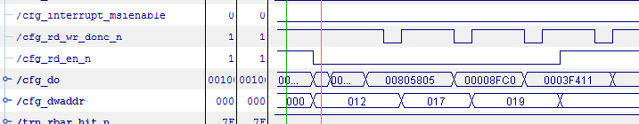
cfg_rd_wr_done_n validates output on cfg_do when asserted low. cfg_dwaddr is address of config space registe being accessed in DWORDS. So address of 012 is 0x048, which is origin of MSI capability record, and 0x00805805 is value of that register being read. The 05 in LSbs is MSI capability Id. Just few para above attempt to read MSI capability returned zero there. Next 58 is pointer to the next record and seems valid, but it was zero in attempt to read this capability before. Within 0080 th only bit asserted is capability to generate 64-bit addresses. The LSb of that field is exactly msiEn bit and it remains zero, i.e. capability was not activated.
Access to 017 (0x5C) is PCIe capability and seems malformed, as C0 capability Id seems to be invalid. Access to 019 (0x64) is to PCIe Link capabilities and values there seems reasonable.
So after all, my major problem is that I cannot activate MSI in FPGA, as it seen from MSI capapability output and from cfg_interrupt_msienable signal. ANother concern is that Pcie_readRegs() seems to not trigger actual reads on the endpoints.
Please comment or suggest, what else to check. Would appreciate any hint.
Thanks in advance.

