Because of the Thanksgiving holiday in the U.S., TI E2E™ design support forum responses may be delayed from November 25 through December 2. Thank you for your patience.

This thread has been locked.

If you have a related question, please click the "Ask a related question" button in the top right corner. The newly created question will be automatically linked to this question.

PCIe Endpoint Configuration space layout

Hello,

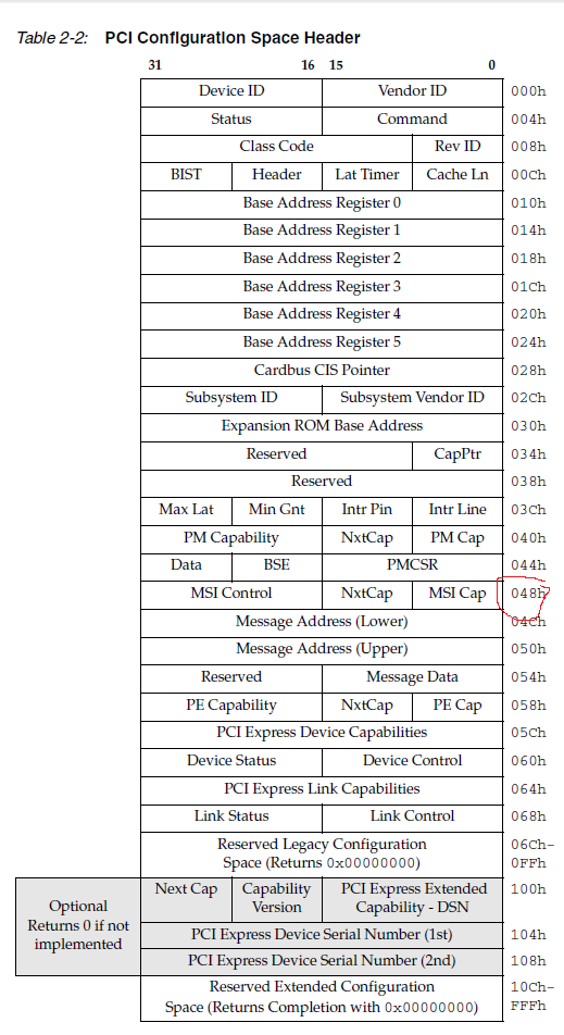
I am working to connect C6670 to Spartan6 FPGA over PCIe. One trouble I see was behaviour of configuration space accesses. I have just realized, that configuration space layout is coded differently in DSP and FPGA. As per FPGA, Xilinx UG654 defines PCI configuration header as follows:

Please note, that at 0x34 there is s capability pointer, which points to PM Cap at 0x40, which in turn points to 0x48, where MSI Cap is located. The numbers in NxtCap pointers do agree with expected when I dump complete config space of FPGA.

When playing with MSI capability from DSP side, I have noticed, that msiEn bit was written to wrong location. While I expected it to go to config register at 0x48, the bit appeared in register at 0x50. There is no surprise, that FPGA does not operate properly with such a setting. Then I traced PCIe endpoint config space layout in pdk_C6670_1_1_2_6\packages\ti\csl\cslr_pcie_cfg_space_endpoint.h. Particularly, please see the following:

typedef struct  {
    volatile Uint32 VENDOR_DEVICE_ID;
    volatile Uint32 STATUS_COMMAND;
    volatile Uint32 CLASSCODE_REVID;
    volatile Uint32 BIST_HEADER;
    volatile Uint32 BAR[6];
    volatile Uint32 CARDBUS;
    volatile Uint32 SUBSYS_VNDR_ID;
    volatile Uint32 EXPNSN_ROM;
    volatile Uint32 CAP_PTR;
    volatile Uint8 RSVD0[4];
    volatile Uint32 INT_PIN;
    volatile Uint32 PMCAP;
    volatile Uint32 PM_CTL_STAT;
    volatile Uint8 RSVD1[8];
    volatile Uint32 MSI_CAP;
...
} CSL_Pcie_cfg_space_endpointRegs;

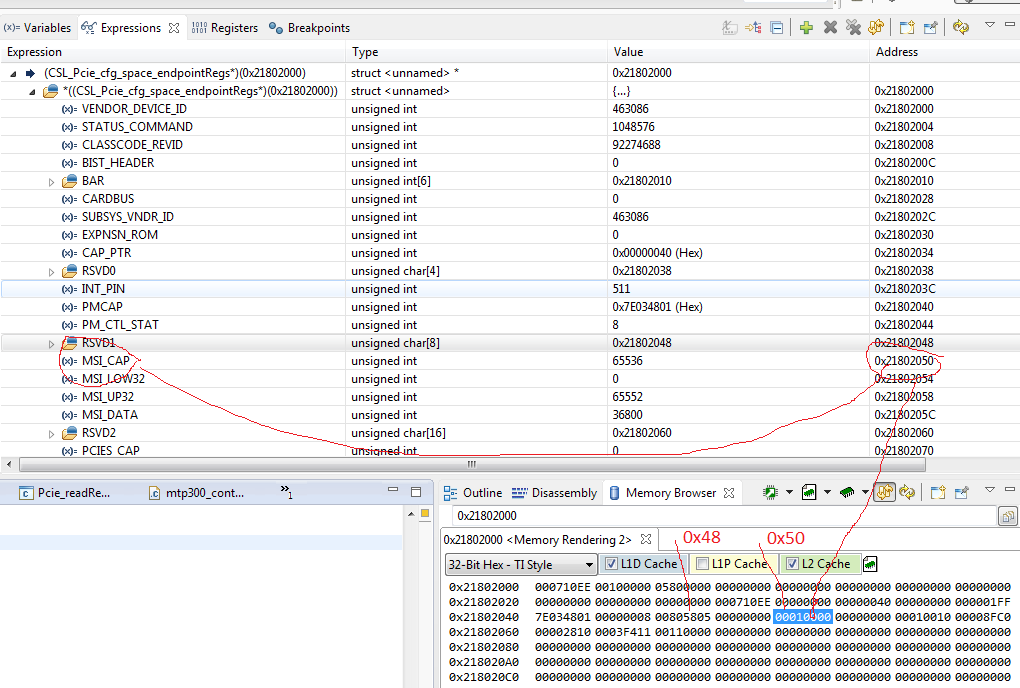
Please notice there are 8 bytes (=2 DWORDS) of RSVD1 between  PM_CTL_STAT and MSI_CAP fields. There is no such a reserved space in Xilinx FPGA. Because of that FPGA expects MSI capabilities to exist at 0x48, but DSP writes them to 0x50. One can see that in the following sreenshot

I have just executed the line

setRegs.msiCap  = &MsiCap;
MsiCap.msiEn    = 1;
if ( pcie_RET_OK !=  Pcie_writeRegs(handle, pcie_LOCATION_REMOTE, &setRegs) )...

I expected value of 0x00010000 to be written over 0x48, but in fact that value was written to 0x50.

So the definition of endpoint address space in CSL does not match layout of actual config space in FPGA.


I'm afraid, I cannot use relevant part of PCIe LLD because of the above mentioned discrepancy, so have to write my own code to handle FPGA, but just wonder, what is rationale of having config space defined with reserved gaps, as in CSL?

  • Hi,

    Please refer "Chapter 3 Registers" PCIe user guide document(SPRUGS6D). This chapter describes the PCI Express registers. The offset is relative to the associated base address of the module. See the device-specific data manual for the memory address of these registers.

    Thanks,
  • Hello,

    I believe support forum is not only RTFM place, so let me give an answer which might be useful for other readers.

    As per PCIe spec, the only portion of configuration space guaranteed to be same across all devices is configuration header, ranging to 0x3C, namely "PCI 3.0 Compatible Configuration Space Header". The rest of the config space is available through mechanism of capabilities linked list. Particularly, bit 4 in Status register (offset 0x06), or equivalently bit 19 in StatusCommand at 0x04 indicates presence of capabilities list. Because all PCIe devices have to implement at least PCIe capabilities record, this bit is always on.

    Next, CapPtr field at 0x34 points to the first item in capabilities linked list. Each record in that list implements CapId, NxtCap fields and capability register itself. Through this mechanism multiple capabilities can be defined.

    The most important point behind that is the only fixed location is CapPtr field at 0x34. Records of the actual capabilities can have variable location. Normally, operating system traverses trough the linked list during enumeration process and builds its view of remote device capabilities.

    Now returning back to the original post, one may see, that both Xilinx and TI ways to define configuration space layout are compliant. Just incompatible with each other.

    Knowing all that, the developer should know, that CSL is good to work only against another TI DSP. With other devices there might be incompatibilities. Then one should refrain from using TI's PCIe CSL and LLD, and develop own code, which match remote device layout. This is particularly true with Spartan 6 FPGA from Xilinx, and their Virtex 6 AFAIK.

    Hope this would save someone weeks of fruitless search.

  • Thanks for your detailed information. It should be useful for other community members.