This thread has been locked.

If you have a related question, please click the "Ask a related question" button in the top right corner. The newly created question will be automatically linked to this question.

GPMC Synchronous Access on AAD device, address stuck at 0

Other Parts Discussed in Thread: AM3359

I have a problem setting up the GPMC for synchronous access on a AAD device (an FPGA).

Asynchronous access works fine with these register settings:

WR_MEM_32(GPMC_CONFIG1(FPGA_GPMC_CS), 0x00001100);
WR_MEM_32(GPMC_CONFIG2(FPGA_GPMC_CS), 0x00060A00);
WR_MEM_32(GPMC_CONFIG3(FPGA_GPMC_CS), 0x11030302);
WR_MEM_32(GPMC_CONFIG4(FPGA_GPMC_CS), 0x05044804);
WR_MEM_32(GPMC_CONFIG5(FPGA_GPMC_CS), 0x0008060A);
WR_MEM_32(GPMC_CONFIG6(FPGA_GPMC_CS), 0x06040000);
WR_MEM_32(GPMC_CONFIG7(FPGA_GPMC_CS), 0x00000010);

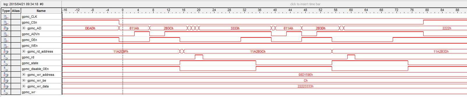
But as soon as I change the read and write type bits to 1 (synchronous access), I can see the clock being enabled during access, but the address/data lines always stay at 0x0000 (data during write access is set properly, and also data is read - though both will obviously only work on address 0).

WR_MEM_32(GPMC_CONFIG1(FPGA_GPMC_CS), 0x28001100);
WR_MEM_32(GPMC_CONFIG2(FPGA_GPMC_CS), 0x00060A00);
WR_MEM_32(GPMC_CONFIG3(FPGA_GPMC_CS), 0x11030302);
WR_MEM_32(GPMC_CONFIG4(FPGA_GPMC_CS), 0x05044804);
WR_MEM_32(GPMC_CONFIG5(FPGA_GPMC_CS), 0x0008060A);
WR_MEM_32(GPMC_CONFIG6(FPGA_GPMC_CS), 0x06040000);
WR_MEM_32(GPMC_CONFIG7(FPGA_GPMC_CS), 0x00000010);

Am I doing something wrong / missing some crucial things?
Thank You in advance for any helpful answers.

  • Hi,

    Which processor is this? What is the software that you use?

  • Sorry, i totally forgot to mention that. It's an AM3359 and I'm using CCS 6.
    I'm running the initialisation via GEL file and then access the "memory" (Cyclone V FPGA) via CCS 6 Memory Viewer.
    I can monitor the actual access patterns via Signal Tap through the FPGA.

  • Do you enable the CS before writing: CSVALID=1 (bit 6 in GPMC_CONFIG7)?

  • Yes of course. I also implemented the configurations as menu scripts, so I can change configuration on the fly.
    However, when I use the "synchronous" configuration, I can see the GPMC_CLK being enabled (which is to be expected), but the GPMC_AD lines remain at the same value (either 0 or as in the pictures below at the value of the MSB address word) during the first and second address phases - data (in case of write access) is output correctly though.

    This is the complete GEL file script (as far as it regards GPMC configuration):

    /* GPMC */

    menuitem "GPMC"

    #define FPGA_GPMC_CS                2

    FPGA_GPMC_Config()
    {
        GEL_TextOut("FPGA GPMC configuration is in progress ....... \n","Output",1,1,1);
        FPGA_GPMC_Config_PinMux();
        FPGA_GPMC_Config_Register_Asynchronous();
        GEL_TextOut("FPGA GPMC configuration is done \n","Output",1,1,1);
    }

    hotmenu FPGA_GPMC_Config_PinMux()
    {
        GEL_TextOut("FPGA GPMC PinMux configuration is in progress ....... \n","Output",1,1,1);

        WR_MEM_32(CONF_GPMC_CSn0,    0x20);    // CSn0
        WR_MEM_32(CONF_GPMC_CSn1,    0x21);    // CLK
        WR_MEM_32(CONF_GPMC_CSn2,    0x20);    // CSn2

        WR_MEM_32(CONF_GPMC_WEn,    0x20);    // WEn
        WR_MEM_32(CONF_GPMC_OEn_REn,    0x20);    // OEn_REn
        WR_MEM_32(CONF_GPMC_ADVn_ALE,    0x20);    // ADVn_ALE

        WR_MEM_32(CONF_GPMC_AD0,    0x20);    // AD0
        WR_MEM_32(CONF_GPMC_AD1,    0x20);    // AD1
        WR_MEM_32(CONF_GPMC_AD2,    0x20);    // AD2
        WR_MEM_32(CONF_GPMC_AD3,    0x20);    // AD3
        WR_MEM_32(CONF_GPMC_AD4,    0x20);    // AD4
        WR_MEM_32(CONF_GPMC_AD5,    0x20);    // AD5
        WR_MEM_32(CONF_GPMC_AD6,    0x20);    // AD6
        WR_MEM_32(CONF_GPMC_AD7,    0x20);    // AD7
        WR_MEM_32(CONF_GPMC_AD8,    0x20);    // AD8
        WR_MEM_32(CONF_GPMC_AD9,    0x20);    // AD9
        WR_MEM_32(CONF_GPMC_AD10,    0x20);    // AD10
        WR_MEM_32(CONF_GPMC_AD11,    0x20);    // AD11
        WR_MEM_32(CONF_GPMC_AD12,    0x20);    // AD12
        WR_MEM_32(CONF_GPMC_AD13,    0x20);    // AD13
        WR_MEM_32(CONF_GPMC_AD14,    0x20);    // AD14
        WR_MEM_32(CONF_GPMC_AD15,    0x20);    // AD15
        
        GEL_TextOut("FPGA GPMC PinMux configuration done \n","Output",1,1,1);
    }

    hotmenu FPGA_GPMC_Config_Register_Asynchronous()
    {
        UWORD32 temp;
        
        GEL_TextOut("FPGA GPMC Register configuration (asynchronous) is in progress ....... \n","Output",1,1,1);
        
        // Clear CSVALID
        temp = RD_MEM_32(GPMC_CONFIG7(FPGA_GPMC_CS));
        temp = temp & ~(1 << 6);
        WR_MEM_32(GPMC_CONFIG7(FPGA_GPMC_CS), temp);
        
        // AM339x GPMC Config Registers
        WR_MEM_32(GPMC_CONFIG1(FPGA_GPMC_CS), 0x00001100);
        WR_MEM_32(GPMC_CONFIG2(FPGA_GPMC_CS), 0x00060A00);
        WR_MEM_32(GPMC_CONFIG3(FPGA_GPMC_CS), 0x11030302);
        WR_MEM_32(GPMC_CONFIG4(FPGA_GPMC_CS), 0x05044804);
        WR_MEM_32(GPMC_CONFIG5(FPGA_GPMC_CS), 0x0008060A);
        WR_MEM_32(GPMC_CONFIG6(FPGA_GPMC_CS), 0x06040000);
        WR_MEM_32(GPMC_CONFIG7(FPGA_GPMC_CS), 0x00000010);
        
        // Set CSVALID
        temp = RD_MEM_32(GPMC_CONFIG7(FPGA_GPMC_CS));
        temp = temp | (1 << 6);
        WR_MEM_32(GPMC_CONFIG7(FPGA_GPMC_CS), temp);
        
        GEL_TextOut("FPGA GPMC Register configuration (asynchronous) done \n","Output",1,1,1);
    }

    hotmenu FPGA_GPMC_Config_Register_Synchronous()
    {
        UWORD32 temp;
        
        GEL_TextOut("FPGA GPMC Register configuration (synchronous) is in progress ....... \n","Output",1,1,1);
        
        // Clear CSVALID
        temp = RD_MEM_32(GPMC_CONFIG7(FPGA_GPMC_CS));
        temp = temp & ~(1 << 6);
        WR_MEM_32(GPMC_CONFIG7(FPGA_GPMC_CS), temp);
        
        // AM339x GPMC Config Registers
        WR_MEM_32(GPMC_CONFIG1(FPGA_GPMC_CS), 0x28001100);
        WR_MEM_32(GPMC_CONFIG2(FPGA_GPMC_CS), 0x00060A00);
        WR_MEM_32(GPMC_CONFIG3(FPGA_GPMC_CS), 0x11030302);
        WR_MEM_32(GPMC_CONFIG4(FPGA_GPMC_CS), 0x05044804);
        WR_MEM_32(GPMC_CONFIG5(FPGA_GPMC_CS), 0x0008060A);
        WR_MEM_32(GPMC_CONFIG6(FPGA_GPMC_CS), 0x06040000);
        WR_MEM_32(GPMC_CONFIG7(FPGA_GPMC_CS), 0x00000010);
        
        // Set CSVALID
        temp = RD_MEM_32(GPMC_CONFIG7(FPGA_GPMC_CS));
        temp = temp | (1 << 6);
        WR_MEM_32(GPMC_CONFIG7(FPGA_GPMC_CS), temp);
        
        GEL_TextOut("FPGA GPMC Register configuration (synchronous) done \n","Output",1,1,1);
    }


    This is an asynchronous access to address 0x12345678 (16-bit address of the device: 0x011A2B3C):

    And this is the same access to address 0x12345678 (16-bit address of the device: 0x011A2B3C) when the synchronous bits are set:

    (In this case the LSB address word remains at the same value as the MSB address word).

  • Yes, I disable the CSVALID bit prior to configuration of the registers and set it afterwards.
    Also the interface is not in use when I clear the CSVALID bit.
  • Checkout this thread for AAD Synchronous configuration that worked for us: e2e.ti.com/.../387016
  • Hi Felix,

    I'm sorry for interrupting.

    I'm having exactly the same problem with AM437x GPMC sync AAD multiplex mode.
    Did you solve the problem?
    If yes, can you give me an advise how you solved it?

    best regards,
    g.f.
  • Unfortunately, I never received any proper help from TI with this matter, neither could I find a "real" solution on my own - I decided to use the asynchronous mode instead (as a workaround as I was running out of time):
    I'm sampling the incoming signals with 200 MHz within the FPGA, which worked for me (as the GPMC clock isn't always running, I did that already anyways).
    I also managed to implement multiple read (burst / page read). Only downside is, I can't implement multiple write (burst write) access that way.

    In case You find a solution, I would be glad if You share it with me. I'll probably try to investigate this matter when I've got some spare time, as multiple write access would decrease the data transfer time from DSP to FPGA alot.

    Kind regards,
    ~ Felix

  • Hi Felix,

    Thank you for the reply.
    I understood. If I found a solution, I will get back to you.

    best regards,
    g.f.
  • Hi Felix, I would first try to get things working at a slower speed (ie, GPMCFCLKDIVIDER=3, for 25MHz), to ensure you have all of your timings proportional. All your adjustments to the timings should scale relative to that once you start speeding the interface up.
    For burst writes, your goal is to try to mimic the timing in Figure 7-23 of the TRM, esp. the ADV and OE signals. Then ensure that WRDATAONADMUXBUS is appropriately scaled to give enough time for the address cycles. Then ensure your bursts are working during the data phase.

    After changing to slower speed, i would make OEAADMUXONTIME a min of 2 until you get things working. Adjust the other OE and ADV timings accordingly (again, refer to Figure 7-23).

    Once writes are working, try to get reads working using similar methods. There isn't a diagram in the TRM for AAD sync burst reads, but the config is similar. Once you get read/writes working at 25MHz, change to 50MHz and retest and confirm the waveforms. Then you can move to 100MHz.

    Regards,
    James