This thread has been locked.

If you have a related question, please click the "Ask a related question" button in the top right corner. The newly created question will be automatically linked to this question.

TPS65217 vdds leakage current

Revision H of "Powering the AM335x with the TPS65217x" moved VDDS from LDO3 to LDO1 when using DDR3(L), and this change was also implemented in BeagleBone Black (rev A6A) with the comment:

This change was based on an alert we just received from TI that there is a power sequencing issue with the TPS65217C power management IC and the power sequencing is incorrect. This change connects the VDDS rail to the VRTC rail. We do not believe at this time, that the issue is causing any issues with the boards, but we want to comply with the directive.

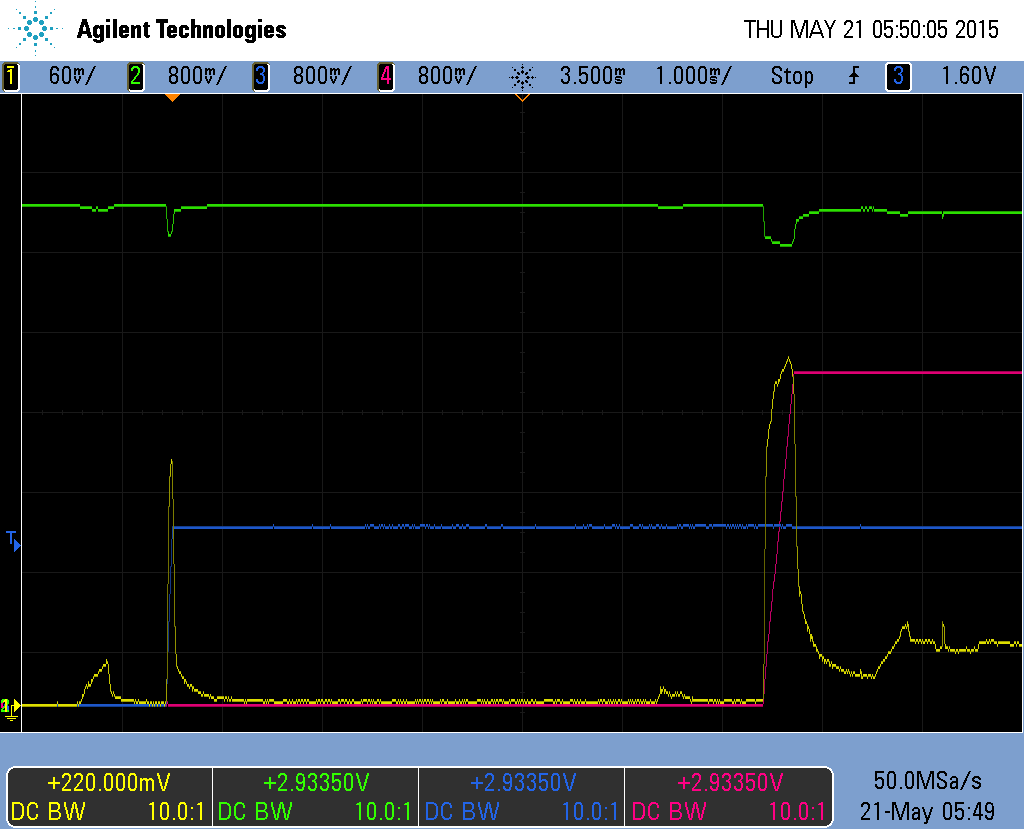
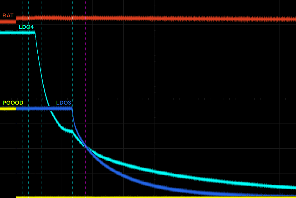
I've been investigating power management on the BBB in detail (mostly in relation to its 3v3b-regulator bug), and along the way noticed that during shutdown the 3v3 rail (LDO4) leveled off at around 1.3V until LDO1 shuts off at strobe 15, after which it would finally start to drop to zero.

This shows various PMIC terminals on a BBB (patched to fix the 3v3b-issue) during an ACTIVE-to-OFF transition (while powered through BAT using a variable PSU at 3.6V):

Note the supply rail dip once the 1.8V rails begin to leak to the 3.3V rail, and the sudden jump upward at strobe 15 indicating significant current was flowing through LDO1 at the time it was shut off. In fact, if a transition into SLEEP-state is done, the 3.3V rail remains at 1.3V indefinitely and the BAT current measured in this state was quite significant (iirc ~ 45 mA).

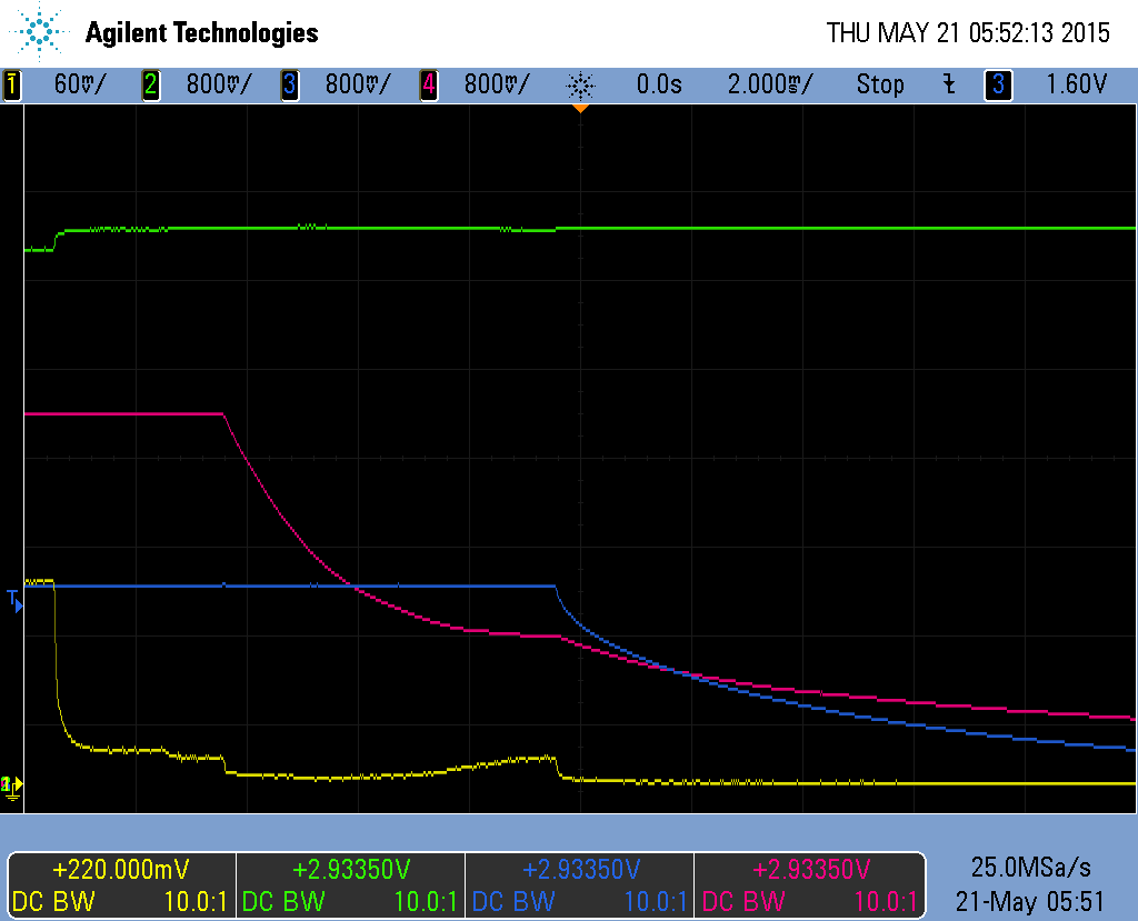
As experiment, VDDS was reconnected to LDO3 instead of LDO1 (by moving resistor R8 to R9). I did not notice any difference during powerup, but shutdown changed significantly:

Leakage evidently still occurs, but the duration of this situation appears substantially reduced. Transition to SLEEP-state (RTC-only sleep) in this case works normally, and produces essentially the same plot as the transition to OFF-state depicted above (since LDO1 wasn't included in these measurements).

So this leaves me with a few questions:

What exactly was the motivation to move VDDS from LDO3 to LDO1?  It seems to me that any undesirable current flow resulting from the late startup or early shutdown of VDDS would have to be occurring between strobes 1 and 2, from VDDS_DDR to VDDS, but I see no evidence of such flow: the current consumption pattern (as estimated by power supply fluctuations) during powerup appears unaffected by moving VDDS, and strobe 1 has no visible effect on the LDO3 voltage during powerup or shutdown.  However, since I do not have measurements of all rails nor accurate current measurements I may be overlooking something.

Why does the VDDS-to-VDDHV leakage only seem to occur on shutdown, and not on powerup?  Unlike the other supply rails it is not really clear at all what the purpose of VDDS is, and I have trouble constructing a mental model of what is going on here.

Given such asymmetry between powerup and shutdown, might it make sense to alter the PMIC sequencer settings prior to initiating shutdown?

  • Hi Matthijs,

    I will ask the factory team what's the reasoning behind this change.

  • Matthijs van Duin said:
    What exactly was the motivation to move VDDS from LDO3 to LDO1?  

      VDDS is one of power supplies used for DDR IO and dual voltage IO. It should be enabled and become stable before enabling VDDS_DDR and VDDSHVx power supplies. LDO3 is enabled after DCDC1 (VDDS_DDR) so cannot be used for powering VDDS. LDO1 comes up before both VDDS_DDR and VDDSHVx power supplies so VDDS should be connected to LDO1 to satisfy AM335x power up sequence requirements. 

    Link to AM335x power requirements in the datasheet

    www.ti.com/.../power_and_clocking

  • Kazunobu Shin said:
    VDDS is one of power supplies used for DDR IO and dual voltage IO. It should be enabled and become stable before enabling VDDS_DDR and VDDSHVx power supplies. LDO3 is enabled after DCDC1 (VDDS_DDR) so cannot be used for powering VDDS. LDO1 comes up before both VDDS_DDR and VDDSHVx power supplies so VDDS should be connected to LDO1 to satisfy AM335x power up sequence requirements.

    This does not really address any of my questions or concerns.

    I am of course aware of the advised power sequence, and had in my original post already concluded the purpose of the change was to reorder VDDS w.r.t. VDDS_DDR. However, given that this demolishes the ability to enter RTC-only sleep, a bit more comment on why exactly this change is necessary would be appropriate I think, especially since:

    1. During my examinations of power-up/down behaviour, I have not witnessed any evidence that connecting VDDS to LDO3 causes any undesirable behaviour.

    2. I however have witnessed undesirable behaviour as a result of connecting VDDS to LDO1.

    My original post already explained these points, but I will elaborate on them using some current measurements I've done recently. (The hardware is a BeagleBone Black rev C patched to support RTC-only sleep: the separate 3V3B-regulator was removed and the 3.3V supplies tied together, VDDS was reconnected to LDO3 instead of LDO1.)

    Legend for scope pics:
    yellow = current (via 0.47Ω 10%, hence approx 128 mA per grid line, 32 mA per minor division)
    green = SYS
    blue = LDO3 (1.8V supplies including VDDS)
    pink = LDO4 (3.3V supplies including VDDHVx)

    For the first point, here's a close-up of power-on sequencing (strobes 1-5):

    The region of interest is on the left between strobes 1 and 2, since this is the 1ms window in which the official power sequencing is being violated. However, after DCDC1 has charged up VDDS_DDR, current falls back towards negligible. In particular, apparently no undesirable current flows as a result of this. Of course it's still possible there might be a problem with voltage-induced stress, although typically there would be protection diodes guarding against this (hence current flow would be visible).

    For the second point, here is a close-up of entry into SLEEP-state:

    Note that current consumption initially drops to negligible once the 3.3V supplies are cut, but when they drop significantly below the 1.8V supplies current increases again and the 3.3V supplies are prevented from falling much lower. Once the 1.8V supplies are cut, the current stops and both supplies begin to drop towards zero. This is clear evidence of heavy leakage occuring from the 1.8V supplies to the 3.3V supplies. When entering OFF-state the same thing is visible, except current consumption needs to be read from the falling slope of SYS since the power path is already disabled at strobe 7.

    As explained in my original post, if VDDS is moved to LDO1, this situation persists until strobe 15 (hence indefinitely if one enters SLEEP-state). This clearly shows that the current flows via VDDS. Since the function of VDDS is still unclear, I do not know which path(s) this current might be taking, but normally I would expect such heavy current flow between separate power supply rails to be undesirable. In this case the current appears to be about 35 mA, but it will depend on how much current is drawn from the 3.3V supplies and I've seen worse (i.e. closer to the max rating of VDDS).

    P.S. I've noticed this topic has been moved from the PMU forum to the Sitara forum. It would have been polite if some kind of notice had been given of this.