This thread has been locked.

If you have a related question, please click the "Ask a related question" button in the top right corner. The newly created question will be automatically linked to this question.

EDMA 3

Other Parts Discussed in Thread: TMS320C6424

Hi.

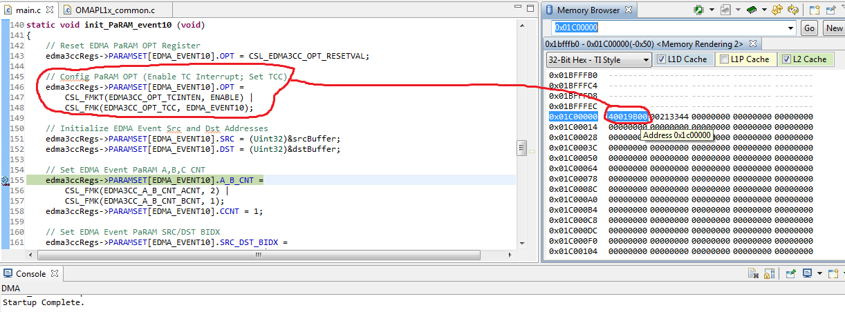
I am using EDMA_event_trig_dspL137 example for my C6745 board. It is work ok.

But I don't understand the next:


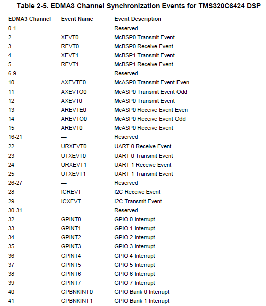
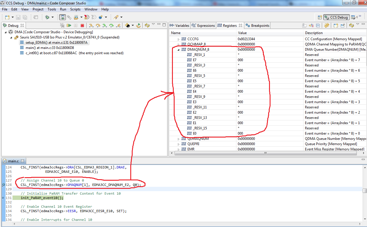
 1) CSL_FINST(edma3ccRegs->DRA[CSL_EDMA3_REGION_1].DRAE, EDMA3CC_DRAE_E10, ENABLE); // Enable Channel 10 to DSP (Region 1)

I don't understand why Channel number is 10   -> [DRAE_E10].

For example I want using McASP0 with EDMA, what channel number must be ?

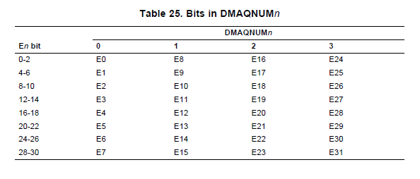
2)  CSL_FINST(edma3ccRegs->DMAQNUM[1], EDMA3CC_DMAQNUM_E2, Q0);  // Assign Channel 10 to Queue 0

I don't understand this entry: EDMA3CC_DMAQNUM_E2, Q0. Why E2 ?

I am reading sprufl1c document, but i am find only the next information:

Thanks.

  • I am find EDMA3 Channel Synchronization Events table for TMS320C6424 DSP in SPRUEM5A, but i can not find this information in sprufl1c for C6745 DSP. Where i can find this information?
    Thanks.

  • Hi Alex,
    You will find these information in C6745 datasheet (SPRS377F).
    Please check Table 6-16 on page 86.
    Below mentioned is the link to find datasheet for C6745.
    www.ti.com/.../tms320c6745.pdf
  • Ok, thanks.

    I don't understand the next:

    CSL_FINST(edma3ccRegs->DMAQNUM[1], EDMA3CC_DMAQNUM_E2, Q0);  // Assign Channel 10 to Queue 0

    Why  all  EDMA3CC_DMAQNUM  values  are zero ?

    Is it correct ?

    Thanks.

  • Alex,

    The EDMA3 User Guide that you have been referencing has very good explanations of all the components of the Channel Controller (CC) and the Transfer Controller (TC). It discusses the available queues and the fact that you can select a queue for each channel using the DMAQNUMn registers as you have been practicing here.

    In your code, you have comments referring to Channel 10 but your code has been edited to use E2 which is for Channel 2. Getting these to match is not vital to your code working but it will make it very difficult for you to keep everything in order, I fear.

    In SPRUFL1c, you can look at the DMAQNUMn registers to see what their default reset values are. These are probably 0. If you use the code that you have circled in red above, what value would you expect to be written into the DMAQNUM register in the field for E2?

    Balancing the allocation of channels to queues can help with optimizing the performance of an application that uses a lot of DMA channels for many purposes. All of the channels allocated the Queue0 will run sequentially with each other, if several of those channels are trigger at about the same time. But if two channels are allocated to different queues, then those channels can run simultaneously. This can lead to better performance.

    For most applications, it will not matter and you can leave all the queues at 0. Especially when you are starting off with your work on the EDMA3 functionality, it will be easiest to ignore the queue number and get the DMA functionality working.

    Regards,
    RandyP
  • Ok, Thank You, Randy.

    I am find the next example  "c6747_audio_edma_v4.zip"  -

    I want modify this example for my DSK, but there is a "lack of understanding" about how it works.

    #define EDMA_XMTPING         32

    #define EDMA_XMTPONG         33

    #define EDMA_RCVPING         34

    #define EDMA_RCVPONG         35

    // 1. setup channel PaRAM slot

       param.OPT = (EDMA_XMT_PING_TCC << 12) | (1 << 20);      // transfer complete interrupt enabled

       param.SRC = (Uint32)src_ping_L;

       param.A_B_CNT = (2 << 16) | sample_size;                // actual format: BCNT|ACNT

       param.DST = (Uint32)dst;

       param.SRC_DST_BIDX = (0 << 16) | ping_offset;           // actual format: DSTBIDX|SCRBIDX

       param.LINK_BCNTRLD = (2 << 16) | (EDMA_XMTPONG * 0x20); // actual format: BCNTRLD|LINK

       param.SRC_DST_CIDX = (0 << 16) | (ping_c_idx & 0x0000FFFF); // actual format: DSTCIDX|SRCCIDX

       param.CCNT = sample_count;

       edmaWritePaRAM(EDMA_MCASPTXCH, &param);

    1) Why    EDMA_XMTPING   ->  32,  EDMA_XMTPONG  ->  33    etc.  What means these numbers?

    2)  param.LINK_BCNTRLD = (2 << 16) | (EDMA_XMTPONG * 0x20); // actual format: BCNTRLD|LINK

    (EDMA_XMTPONG * 0x20) is a Link Address. 

    0x20 in this entry means 32-byte PaRAM set.  My understanding is correct ? 

    I am reading the next:

    16.2.3.2.12 Link Address (LINK)
    The EDMA3CC provides a mechanism, called linking, to reload the current PaRAM set upon its natural
    termination (that is, after the count fields are decremented to 0) with a new PaRAM set. The 16-bit
    parameter LINK specifies the byte address offset in the PaRAM from which the EDMA3CC loads/reloads
    the next PaRAM set during linking.
    You must program the link address to point to a valid aligned 32-byte PaRAM set. The 5 LSBs of the LINK
    field should be cleared to 0.
    The EDMA3CC ignores the upper 2 bits of the LINK entry, allowing the programmer the flexibility of
    programming the link address as either an absolute/literal byte address or use the PaRAM-base-relative
    offset address. Therefore, if you make use of the literal address with a range from 4000h to 7FFFh, it will
    be treated as a PaRAM-base-relative value of 0000h to 3FFFh.
    You should make sure to program the LINK field correctly, so that link update is requested from a PaRAM
    address that falls in the range of the available PaRAM addresses on the device.

    A LINK value of FFFFh is referred to as a NULL link that should cause the EDMA3CC to perform an
    internal write of 0 to all entries of the current PaRAM set, except for the LINK field that is set to FFFFh.
    Also, see Section 16.2.5 for details on terminating a transfer.

    But I don't understand how works this entry:   EDMA_XMTPONG * 0x20. I do not have a full understanding how linking mechanism works.

    Your help will save me a lot of time.

    Thanks.

  • I find a good explanation for resolving my problem.

    This is article  "StarterWare Audio Application"   .

     In c6747_audio_edma  example we have a similar idea.

     The paRAM set EDMA_RCVPONG is linked to paRAM set EDMA_RCVPING, which is initialized to receive data in rcv_pong. The paRAM set EDMA_RCVPING is linked back to paRAM set EDMA_RCVPONG. Hence the reception paRAM set is initialized as: 

    EDMA_RCVPONG --> EDMA_RCVPING --> EDMA_RCVPONG. 

    My understanding is correct ?

    2) 

    #define EDMA_XMTPING 32
    #define EDMA_XMTPONG 33
    #define EDMA_RCVPING 34
    #define EDMA_RCVPONG 35

    Numbers in this defines can be any  from 0 to 127. Is it correct ?

  • Hi,

    Thanks for your update.

    Yes, your understanding is correct.

    Please find attached the c6748 starterware example code with two buffers (ping, pong) on both tx. and rx. side and accordingly, configure ping pong buffers for 150 stereo samples of 16 or 32 bits/sample

    Kindly check the EDMA ping pong buffer code as below:

    /cfs-file/__key/communityserver-discussions-components-files/791/7851.OMAPL138_5F00_StarterWare_5F00_McASP_5F00_EDMA_5F00_PING_5F00_PONG.zip

    Buffers used in the code are rxbuf_ping, rxbuf_pong, txbuf_ping, txbuf_pong and please check it.

    Thanks & regards,

    Sivaraj K

    -----------------------------------------------------------------------------------------------

    Please click "Verify Answer" button if this post answers your question.

    -----------------------------------------------------------------------------------------------

  • Ok, thank you very much Sivaraj .
    C6748 starterware example code is realy good for quick start.
  • Hi.

    I can't  find  Channel Options Parameter (OPT) register in CCS v5.5 for EDMA 3.

    How to check its parameters on Debug mode ?

    Thanks.

  • Hi Alex,

    You can check for OPT value using exact address of it .
    Check chapter 16 (EDMA3 Controller) of Technical Reference Manual.
    In section 16.4.1 Parameter RAM (PaRAM) Entries are given.

    For OPT offset value is 0h
    and EDMA3CC_0_REGS base address is 0x01C00000u
    As, Physical address = base Address + offset Address
    So you can check OPT value in memory browser at 0x01C00000 itself.
  • Hi Arvind,

    Thanks for your detailed explanation. It's really works, but i have some problem.

    In OPT register I have always value  0x40019B00. (After  reset, after config param OPT etc).

    For example:

    CSL_FMKT(EDMA3CC_OPT_TCINTEN, ENABLE)  ->  set  TCINTEN bit in OPT register.

    But I have the next: 

    0x40019B00_hex  ->   1000000000000011001101100000000_bin  (TCINTEN bit = 0)

    May be I'm doing something wrong?

    Thanks.

  • 0x01C00000  is not OPT address.

    I am find the next:

    Parameter set 10 -> Byte address 0x01C04200

    In Memory  Browser  i have the next:

    It does not correspond to the required values.

    I checked the values of Timer64_P0 registers in memory browser  - it is ok.

    May be I am wrong .

  • Hi Alex,
    Apologies for confusion.
    Yes you are right.
  • Ok, but I don't understand why I have 0xD90DCA03, 0x00364829, 0xE8501A82 etc. values after reset. After reset we must be have 0x00000000 values. Above mentioned values does not correspond to the required values.
  • Alex,

    From what document do you find a requirement that the reset values for the PARAM contents must be 0x00000000? I do not find this anywhere. You can see from your example that this is not a true requirement of the device, so we need to clarify the source of this requirement.

    Regards,
    RandyP
  • Hi Randy.
    Yes you are right. It was my mistake.
    Thanks for your explanation.