This thread has been locked.

If you have a related question, please click the "Ask a related question" button in the top right corner. The newly created question will be automatically linked to this question.

uPP Module Clock Requirements

Other Parts Discussed in Thread: OMAPL138

I wish to use the uPP in receive mode, and am trying to combine the bits and pieces of information from the data sheet (SPRS590F), tech ref (spruh79a), and uPP User's guide(sprugj5b).


Tech Ref, section 6.3.5, on uPP Clocking, tells us that "The uPP subsystem requires a module clock to drive its internal logic"  etc.  Also, "The module clock is always sourced by PLL0_SYSCLK2".  The uPP User’s guide adds the detail that the module clock must be no more than ½ the CPU clock speed.

In the diagrams in the uPP User's guide and in the tech ref, we see a block like this
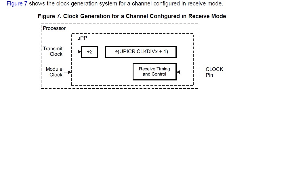
 which shows us the same module clock, along with an input receive clock, and also a transmit clock.  It mentions that the input on CLOCK pin must be at maximum ¼ of the CPU clock speed.

The data sheet sprs590F has detailed timing for the signal on the clock pin relative to the data, but makes no mention of the Module clock.

So … after piecing together the details from these three documents, I am still lacking two bits of information.

1)      Is there any requirements on the module clock relative to the receive clock?  Perhaps it must be twice as fast?

2)      In receive mode, do I need a transmit clock?  From the text, I would think that I do not, but from Figure 7, it seems to hint that I do need it.  If I need it, what is the requirement relative to the module clock and the receive clock on the CLOCK pin?

Thanks

  • Hi,
    Have you referred the Chapter 7.3.5 in OMAPL138 TRM (spruh77a) ?


    2) In receive mode, do I need a transmit clock? From the text, I would think that I do not, but from Figure 7, it seems to hint that I do need it. If I need it, what is the requirement relative to the module clock and the receive clock on the CLOCK pin?

    Tx clock is not required when you operate uPP as RX alone.


    1) Is there any requirements on the module clock relative to the receive clock? Perhaps it must be twice as fast?

    The channel requires an external clock to drive its CLOCK pin. The incoming clock is not divided, and its
    maximum allowed speed is one fourth (¼) the device CPU clock speed.
  • The question still remains unanswered...are there any requirements on the "Module clock" which appears in the Figure 7 of my previous post.  Perhaps it is not needed at all in receive mode?  I cannot find anything written except that the maximum speed of the Module clock is 1/2 the CPU clock.  Is there any minimum?  Is there any relationship required between the speed of this  "Module clock" and the speed of the external clock on the CLOCK pin?

    If nobody at TI knows the answer, it is OK to say so.  It happens.

    Thanks.

  • Hello Michael,

    1. There is no requirement on the module clock in relative to the receive clock. It is not mandatory to keep the module clock be twice fast as receive clock, there is no external control on the module clock as it is directly driven by the PLL0_SYSCLK2. However the module clock would be twice fast if your external receive clock is at maximum allowed speed of one fourth (¼) the device CPU clock speed.

    2. In receive mode of operation, transmit clock is not really required. The block diagram just shows the internal blocks and you can see there is no connectivity between the transmit blocks, ÷2 and ÷(UPICR.CLKDIVx + 1).

    You could also refer section 6.3.5 uPP Clocking in C6748 device TRM for clocking diagram of module clock and transmit clock.

    Hope it clarifies.

    Regards,

    Senthil

  • Hello Michael,

    The data sheet sprs590F has detailed timing for the signal on the clock pin relative to the data, but makes no mention of the Module clock.

    The module clock is intended for internal logic operation of uPP peripheral and the only specification available is the speed cannot be faster than one-half the device CPU clock speed.

    The datasheet have the transmit/receive clock timing relative to the data, as this is considered as IO clock. Since the module clock is internal, it is not shown in the timing diagram.

    Regards,
    Senthil