This thread has been locked.

If you have a related question, please click the "Ask a related question" button in the top right corner. The newly created question will be automatically linked to this question.

Difference of GPMC Interface [XIP] between OMAP35 series and AM335X series...

Hi,

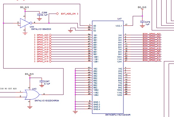
We want to interface between AM335X series processor with parallel NOR Flash from Spansion for which we have an application note attached in this email but this application note refers to OMAP35 series GPMC interface with NOR Flash.

Can we refer the same application note for AM335X series or are there some differences between AM35 and AM33 series of processors as far as GPMC or for that matter XIP interface is concerned. 

Thanking you.

RegardsIface_Flash_TI_OMAP_Proc_AN.pdf

Mohit

  • You should refer to section 26.1.7.2 from the AM335X TRM Rev. L for correct connections.

  • Hi Biser,

    In the table 26-10, it shows that for booting in muxed mode the higher address lines will not be used but only AD bus. Why it is so? We want to use address data multiplexed mode and our 1 Mbit OTP has 17 address lines and 8 bit data bus from ATMEL. For the time being just forget about the spansion Flash described earlier as we will use it only when the booting with OTP is successful.

    Please tell me whether my connection diagram in that case will be correct or not [IN CASE AT ALL IF I CAN USE HIGHER ADDRESS LINES]:-

    uC - AM335X [ZCZ package]

    OTP ADDRESS uC PINNAME[Attributes in DS] GPMC SIGNALS[TABLE 7-5 in TRM]

    A16 GPMC_A1 GPMC_A[1]
    A15-A0 GPMC_AD15-GPMC_AD0 GPMC_AD[15] - GPMC_AD[0]
  • sorry for the bad formatting. PFA essential..

    Please clarify this.

    OTP ADDRESS                uC PINNAME[Attributes in DS]                  GPMC SIGNALS[TABLE 7-5 in TRM]
    
    A16                        GPMC_A1                                       GPMC_A[1]
    A15-A0                     GPMC_AD15-GPMC_AD0                            GPMC_AD[15] - GPMC_AD[0]

  • AD multiplexed mode is not supported for 8-bit devices. With your device you can only boot in one of the XIP modes described in Table 26-9. Pay attention to this:

    "Specifically, external logic is needed to isolate the upper address lines (A12–A27) of the NOR flash from the device pins and drive them low during non-muxed NOR boot."

  • OH!! I have read this fact so many times but I could not gather this due to shuttle between OTP and NOR Flash...

    But this means that only A0 to A11 can be used to address the OTP during boot through the ROM code and rest of the addresses need to be driven through normal GPIOs. Here external logic means mux selection right!!! For driving higher addresses of OTP, GPMC controller cannot be used during boot in case the device is an 8 bit device.

    Kindly revert. Thankful to you.
  • Hi Biser,

    Please revert as to our understanding in the previous post is correct or not. For us external booting is a never earlier done thing and so we are jittery in this zone.

    Regards.

  • MOHIT HADA said:
    But this means that only A0 to A11 can be used to address the OTP during boot through the ROM code

    This is correct.

    MOHIT HADA said:
    rest of the addresses need to be driven through normal GPIOs

    This is not necessary. You need only to ensure that addresses above A11 are low at reset release time, so that the ROM code can start reading from the correct NOR location. The simplest way to do this is through external pulldown resistors. Another way is to use an external switch, controlled through a GPIO. See this schematic to get the idea:

    This is just an example, addresses are different on the picture.

    Then what has to be done is to pinmux the high GPMC address pins within the first 4k of code, after which the whole NOR can be accessed correctly.

  • Hi Biser,

    I have understood your detailed reply and thank you for it. I have attached a revised block diagram of the architecture that we are following and there is an OTP and NOR Flash both are used, as told earlier. Control gets transferred to NOR Flash [1Gbit - 64MX16] after booting has been done using OTP [Earlier 1Mbit - 128KX8 and Now 64KX16 after reading your reply] which checks the content of the Flash. I think if we use OTP 16 bit, we can use the multiplexing feature for both the chips NOR and OTP.

    Sorry for bothering. I will wait for your revert on our block diagram.

    Finally as I write this post will it be better to read the contents of the entire OTP [which consists of boot program and test program for NAND Flash testing] in the uC and then check the contents of the NOR Flash so that CSn lines are toggled only once OR otherwise?

    Hope to close this chain after your reply. Many Regards...

  • I can see no attachment. You can simply drag and drop it in your reply window.

  • Yes, this looks feasible. One important thing though - if you want to boot from the OTP it must be on GPMC_CS0. You seem to have swapped the CS signals.

  • Thanks Biser,

    We have taken care in the schema. This BD is not updated as far as CSn is concerned. Thanks for observation.

    Regards..