Hello.
I had the problem with SDRAM - https://e2e.ti.com/support/dsp/tms320c6000_high_performance_dsps/f/115/t/446811.
I thought that problem was with SDRAM size (I used 256MBit SDRAM but C6745 support only 128MBit memory size).
Now we bought 64MBit SDRAM - AS4C4M16S-7TCN, but it does not solve the problem.
I have the next error message:
C674X_0: GEL Output:
c6747 DSP Startup Sequence
C674X_0: GEL Output: Setup PINMUX Registers...C674X_0: GEL Output: [Done]
C674X_0: GEL Output: PLL Setup Complete
C674X_0: GEL Output: Setup Power Modules (All on)...C674X_0: GEL Output: [Done]
C674X_0: GEL Output: SDRAM Complete
C674X_0: GEL Output:
Startup Complete.
C674X_0: GEL Output:
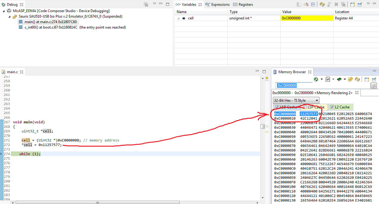
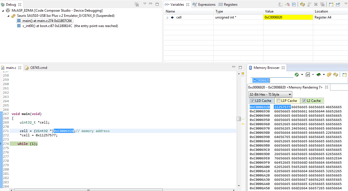
C674X_0: File Loader: Verification failed: Values at address 0x00000000C0006920 do not match Please verify target memory and memory map.
C674X_0: GEL: File: C:\ti\Workspace\McASP_EDMA\Debug\McASP_EDMA.out: a data verification error occurred, file load failed.
I have the next cmd file:
MEMORY
{
DSPL2ROM o = 0x00700000 l = 0x00100000 /* 1MB L2 Internal ROM */
DSPL2RAM o = 0x00800000 l = 0x00040000 /* 256kB L2 Internal RAM */
DSPL1PRAM o = 0x00E00000 l = 0x00008000 /* 32kB L1 Internal Program RAM */
DSPL1DRAM o = 0x00F00000 l = 0x00008000 /* 32kB L1 Internal Data RAM */
SHDSPL2ROM o = 0x11700000 l = 0x00100000 /* 1MB L2 Shared Internal ROM */
SHDSPL2RAM o = 0x11800000 l = 0x00040000 /* 256kB L2 Shared Internal RAM */
SHDSPL1PRAM o = 0x11E00000 l = 0x00008000 /* 32kB L1 Shared Internal Program RAM */
SHDSPL1DRAM o = 0x11F00000 l = 0x00008000 /* 32kB L1 Shared Internal Data RAM */
EMIFACS2 o = 0x60000000 l = 0x02000000 /* 32MB Async Data (CS2) */
EMIFACS3 o = 0x62000000 l = 0x02000000 /* 32MB Async Data (CS3) */
EMIFACS4 o = 0x64000000 l = 0x02000000 /* 32MB Async Data (CS4) */
EMIFACS5 o = 0x66000000 l = 0x02000000 /* 32MB Async Data (CS5) */
EMIFBSDRAM o = 0xC0000000 l = 0x3FFFFFF /* 128MB SDRAM Data */
}
SECTIONS
{
.isr_vectors > EMIFBSDRAM
.text > EMIFBSDRAM
.stack > EMIFBSDRAM
.bss > EMIFBSDRAM
.cio > EMIFBSDRAM
.const > EMIFBSDRAM
.data > EMIFBSDRAM
.switch > EMIFBSDRAM
.sysmem > EMIFBSDRAM
.far > EMIFBSDRAM
.args > EMIFBSDRAM
.ppinfo > EMIFBSDRAM
.ppdata > EMIFBSDRAM
/* COFF sections */
.pinit > EMIFBSDRAM
.cinit > EMIFBSDRAM
/* EABI sections */
.binit > EMIFBSDRAM
.init_array > EMIFBSDRAM
.neardata > EMIFBSDRAM
.fardata > EMIFBSDRAM
.rodata > EMIFBSDRAM
.c6xabi.exidx > EMIFBSDRAM
.c6xabi.extab > EMIFBSDRAM
}
My gel file:
Please tell me where can hide the error.
Thanks.