This thread has been locked.

If you have a related question, please click the "Ask a related question" button in the top right corner. The newly created question will be automatically linked to this question.

AHCLKX for MCASP3 does not output any clock

Guru 20755 points

Hi,

On trying to get mcasp3 to work I am having difficulties.
I have tried many options but all failed..... I don't have MCLK output from mcasp3 AHCLKX pin and I don't understand why....

mcasp2 is getting auxosc->sysclk20->mcasp2_ahclk  and it works OK. now I just wanted to add  auxosc->mcasp3_ahclk

(

mcasp2_ahclk was added with:

clkp_audio_pll = clk_get(NULL,"audio_dpll_clkin_ck");

ret = clk_set_parent(clkp_audio_pll, clkp_osc1);

 clk_put(clkp_audio_pll) ;

)


1. I have verificed that I use the correct pinmux for mcasp3:

MUX_VAL(PINCNTL14, (IEN | IPD | FCN4))  /* MCA[3]_AHCLKX */

2. I have tried to change clocks814_data.c default for mcasp3 parent as following:


static const struct clksel mcasp0to6_auxclk_mux_sel[] = {
{ .parent = &mcasp_auxclk_mux0_ck, .rates = div_1_0_rates },
{ .parent = &audio_dpll_ck, .rates = div_1_1_rates },
{ .parent = &video012_dpll_muxout_ck, .rates = div_1_2_rates },
old:  { .parent = &xref0_ck, .rates = div_1_3_rates },   <-- what is xref0? Can't find it in pll audio schema !
new: { .parent = &audio_dpll_ck, .rates = div_1_1_rates },
{ .parent = &xref1_ck, .rates = div_1_4_rates },
{ .parent = &xref2_ck, .rates = div_1_5_rates },
{ .parent = &osc1_xi_ck, .rates = div_1_6_rates },
{ .parent = NULL}

no clock in mcasp3 AHCLKX
};

3. I have tried to set registers directly, but on reading them I get that value is 0


ioaddr2 = ioremap_nocache(0x481c6000, SZ_1K);
printk("ioaddr2 0x%lx\n",ioaddr2);
*(( unsigned int*) (ioaddr2+0x2d0)) = 0x1;
*(( unsigned int*) (ioaddr2+0x2d4)) = 0x1b0000;
printk("ioaddr reg 0x%x\n",*(( unsigned int*) (ioaddr2+0x2d0))); <-- shows 1 which is OK
printk("ioaddr reg 0x%x\n",*(( unsigned int*) (ioaddr2+0x2d4))); <-- shows 0 while expected 0x1b0000 !!!!!


if (!ioaddr2)
return;
iounmap(ioaddr2);

4. 

I have also tried to change in kernel boot code as following. It did not help.


clkp_osc1 = clk_get(NULL,"osc1_clkin_ck");
clk_rate = clk_get_rate(clkp_osc1);
clk_set_rate(clkp_osc1, 24576000) ;


clkp_audio_pll = clk_get(NULL,"audio_dpll_clkin_ck");
ret = clk_set_parent(clkp_audio_pll, clkp_osc1); //required for mcasp2

clkp_mcasp3 = clk_get(NULL,"davinci-mcasp.3");

ret = clk_set_parent(clkp_mcasp3, clkp_audio_pll);      <------------- return -22 !

 5. I have also validated that the module is ON:

root@dm814x:~# devmem2 0x4818156c
/dev/mem opened.
Memory mapped at address 0x400b9000.
Read at address 0x4818156C (0x400b956c): 0x00000002

 6. also tried to change the registers using devmem2 but it always read back 0 !!

oot@dm814x:~# devmem2 0x481c62d0
/dev/mem opened.
Memory mapped at address 0x40265000.
Read at address 0x481C62D0 (0x402652d0): 0x00000000
root@dm814x:~# devmem2 0x481c62d4
/dev/mem opened.
Memory mapped at address 0x40107000.
Read at address 0x481C62D4 (0x401072d4): 0x00000000
root@dm814x:~# devmem2 0x481c62d4 0xffffffff
/dev/mem opened.
Memory mapped at address 0x40203000.
Illegal data type '0'.
root@dm814x:~# devmem2 0x481c62d4 w 0xffffffff
/dev/mem opened.
Memory mapped at address 0x4008e000.
Read at address 0x481C62D4 (0x4008e2d4): 0x00000000
Write at address 0x481C62D4 (0x4008e2d4): 0xFFFFFFFF, readback 0xFFFFFFFF
root@dm814x:~# devmem2 0x481c62d4
/dev/mem opened.
Memory mapped at address 0x40133000.
Read at address 0x481C62D4 (0x401332d4): 0x00000000
root@dm814x:~#


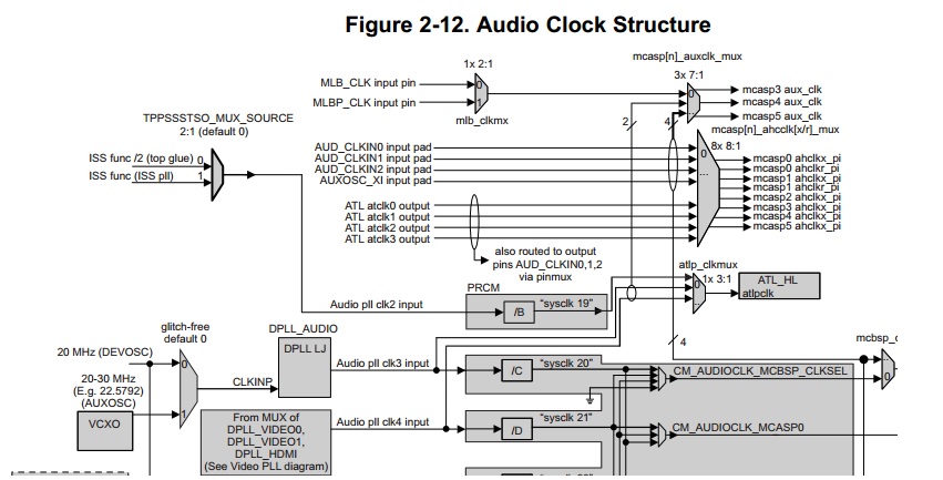
I also don't understand why the default in code is that mcasp3 parent is xref0. I don't see "xref0" in audio pll tree.

 Is there a power mode issue here ? What is wrong with the above ?

Thank you,

Ran

  • Ran,

    Let me clarify first.

    You can export successful clock on the below path:

    auxosc -> sysclk20 -> McASP2 auxclk -> McASP2 AHCLKX_OUT -> H1 pin

    And you need to export clock on the below path?

    auxosc -> sysclk20 -> McASP3 auxclk -> McASP3 AHCLKX_OUT -> L5 pin

    BR
    Pavel
  • Note that McASP2 aux clk (mcasp3_fck) and McASP3 aux clk (mcasp4_fck) have different clock tree path:

    McASP2 aux clk:

    osc1_clkin_ck -> audio_dpll_clkin_ck -> audio_dpll_ck -> sysclk20 -> mcasp3_fck

    McASP3 aux clk:

    osc1_clkin_ck -> audio_dpll_clkin_ck -> audio_dpll_ck -> mcasp4_fck

    McASP2 aux clk is controlled by CM_AUDIOCLK_MCASP2_CLKSEL

    McASP3 aux clk is controlled by McASP345_AUX_CLKSRC[2:0] McASP3_AUX_SOURCE

    So do you need to set this path for McASP3?

    osc1_clkin_ck -> audio_dpll_clkin_ck -> audio_dpll_ck -> mcasp4_fck -> McASP3 AHCLKX_OUT -> L5 pin

    Or you need this path?

    osc1_clkin_ck -> mcasp4_fck -> McASP3 AHCLKX_OUT -> L5 pin

    xref0_ck is AUD_CLKIN0


    BR
    Pavel

  • Ran Shalit said:

    1. I have verificed that I use the correct pinmux for mcasp3:

    MUX_VAL(PINCNTL14, (IEN | IPD | FCN4))  /* MCA[3]_AHCLKX */

    Are you making MCA[3]_AHCLKX input with the IEN flag? Can you check the value of MCA3_AHCLKX/PINCNTL14/0x48140834 register with devmem2 tool?

    BR
    Pavel

  • Hi Pavel,

    I think the only available path I see is 

    osc1_clkin_ck -> audio_dpll_clkin_ck -> audio_dpll_ck -> mcasp4_fck -> McASP3 AHCLKX_OUT -> L5 pin

    and this is what I tried to the in the above trials (which none worked for me).

    I don't see the other path you mentioned: 

    osc1_clkin_ck -> mcasp4_fck -> McASP3 AHCLKX_OUT -> L5 pin

    in the picture below:

    Is there any reason why the above trials did not work ?

    Regards,

    Ran

  • Ok, I understand both path now.

    We actually don't mind the path as long as it gets the 1:1 AUXOSC.

    Thanks,
    Ran
  • Ran,

    Ran Shalit said:

    I don't see the other path you mentioned: 

    osc1_clkin_ck -> mcasp4_fck -> McASP3 AHCLKX_OUT -> L5 pin

    in the picture below

    It is there:

    AUXOSC_XI -> mcasp3 aux_clk

    Ran Shalit said:
    Is there any reason why the above trials did not work ?

    There can be many reasons. Let we start with this one:

    BR
    Pavel

  • Hi Pavel,

    I also tried the other path

    static const struct clksel mcasp0to6_auxclk_mux_sel[] = {

    { .parent = &mcasp_auxclk_mux0_ck, .rates = div_1_0_rates },

    { .parent = &audio_dpll_ck, .rates = div_1_1_rates },

    { .parent = &video012_dpll_muxout_ck, .rates = div_1_2_rates },

       /*  { .parent = &xref0_ck, .rates = div_1_3_rates }, ranranx */

       { .parent = &osc1_clkin_ck, .rates = div_1_1_rates },

       { .parent = &xref1_ck, .rates = div_1_4_rates },

       { .parent = &xref2_ck, .rates = div_1_5_rates },

       { .parent = &osc1_xi_ck, .rates = div_1_6_rates },

    { .parent = NULL}

    };

    But I still don't get the clock in pin5.

    Regards,

    Ran

  • Hi Pavel,


    root@dm814x:~# devmem2 0x48140834
    /dev/mem opened.
    Memory mapped at address 0x400dd000.
    Read at address 0x48140834 (0x400dd834): 0x00040008
    root@dm814x:~#

    Regards,
    Ran
  • Ran Shalit said:

    static const struct clksel mcasp0to6_auxclk_mux_sel[] = {

    { .parent = &mcasp_auxclk_mux0_ck, .rates = div_1_0_rates },

    { .parent = &audio_dpll_ck, .rates = div_1_1_rates },

    { .parent = &video012_dpll_muxout_ck, .rates = div_1_2_rates },

       /*  { .parent = &xref0_ck, .rates = div_1_3_rates }, ranranx */

       { .parent = &osc1_clkin_ck, .rates = div_1_1_rates },

       { .parent = &xref1_ck, .rates = div_1_4_rates },

       { .parent = &xref2_ck, .rates = div_1_5_rates },

       { .parent = &osc1_xi_ck, .rates = div_1_6_rates },

    { .parent = NULL}

    Can you please state why you update the mcasp0to6_auxclk_mux_sel[] ? I do not think this array is wrong and need to be corrected. From where you get information that this array is wrong and need to be corrected?


    BR
    Pavel

  • I also see that it is enabled in our code:

    MUX_VAL(PINCNTL14, (IEN | IPD | FCN4)) /*ranranx FCN4 ))*/ /* MCA[3]_AHCLKX */\

    Regards,
    Ran
  • Ran Shalit said:
    root@dm814x:~# devmem2 0x48140834
    /dev/mem opened.
    Memory mapped at address 0x400dd000.
    Read at address 0x48140834 (0x400dd834): 0x00040008

    Why you set this pin as input, when you need it as an output, to export clock on it from inside the device?

    BR
    Pavel

  • Ran Shalit said:
    I also see that it is enabled in our code:

    MUX_VAL(PINCNTL14, (IEN | IPD | FCN4)) /*ranranx FCN4 ))*/ /* MCA[3]_AHCLKX */\

    Enabled as an input?? Why??

  • Hi Pavel,

    I tried to set mcasp3 parent clock as osc1_clkin_ck using these array.
    I understand from you that this wrong doing, therefore I will remove this patch (it does not work anyway)

    Regards,
    Ran
  • Hi Pavel,

    Thank you very much for the assistance.

    Do you mean we need to remove the IEN flag ? (received enabled)

    I see that we defined the same way both MCA[2]_AHCLKX (which works) and MCA[3]_AHCLKX :

    MUX_VAL(PINCNTL14, (IEN | IPD | FCN4)) /* MCA[3]_AHCLKX */\
    MUX_VAL(PINCNTL16, (IEN | IPD | FCN3 )) /* MCA[2]_AHCLKX */\

    Regards,
    Ran
  • Ran Shalit said:
    I tried to set mcasp3 parent clock as osc1_clkin_ck using these array.

    You need to set mcasp3 parent clock as osc1_xi_ck, not as osc1_clkin_ck. osc1_xi_ck is AUXOSC_XI/AUXOSC_MXI, osc1_clkin_ck is AUX_CLKIN. See DM814x TRM and datasheet for more info.

    BR
    Pavel

  • Ran Shalit said:
    Do you mean we need to remove the IEN flag ? (received enabled)

    yes

    You should have 0x00080008 value in MCA3_AHCLKX/PINCNTL14/0x48140834 register.

    BR
    Pavel

  • Ran Shalit said:
    I see that we defined the same way both MCA[2]_AHCLKX (which works) and MCA[3]_AHCLKX :

    MUX_VAL(PINCNTL14, (IEN | IPD | FCN4)) /* MCA[3]_AHCLKX */\
    MUX_VAL(PINCNTL16, (IEN | IPD | FCN3 )) /* MCA[2]_AHCLKX */\

    May be you are getting clock on the MCA[2]_AHCLKX input, not export clock to the MCA[2]_AHCLKX output.

  • Hi Pavel,

    Should we remove IEN:
    MUX_VAL(PINCNTL14, ( IPD | FCN4)) /* MCA[3]_AHCLKX */\
    MUX_VAL(PINCNTL16, ( IPD | FCN3 )) /* MCA[2]_AHCLKX */\
    ?

    Regards,
    Ran
  • Hi Pavel,

    I've removed IEN:

    MUX_VAL(PINCNTL14, ( IPD | FCN4)) /* MCA[3]_AHCLKX */\
    MUX_VAL(PINCNTL16, ( IPD | FCN3 )) /* MCA[2]_AHCLKX */\

    root@dm814x:~# devmem2 0x48140834

    /dev/mem opened.

    Memory mapped at address 0x4018c000.

    Read at address  0x48140834 (0x4018c834): 0x00000008

    root@dm814x:~#

    But I still don't have clock in MCA[3]_AHCLKX

    Regards,

    Ran

  • I have configured it now as following:

    root@dm814x:~# devmem2 0x48140834

    /dev/mem opened.

    Memory mapped at address 0x400ee000.

    Read at address  0x48140834 (0x400ee834): 0x00080008


    Regards,

    Ran


  • Hi Pavel,

    Are there any additional changes that we need to do except for 0x48140834 register ?

    I've tried again the changes which I posted in the original post (above), but I still fail to get clock in MCA[3]_AHCLKX

    I am trying to use the following path:
    osc1_clkin_ck -> audio_dpll_clkin_ck -> audio_dpll_ck -> mcasp4_fck -> McASP3 AHCLKX_OUT -> L5 pin

    As to AUXOSC_XI we are not sure if it means the same as AUXOSC clock (if it is the same, then that path can be used if the first one does not work)

    Thank you,
    Ran
  • I think that the problem is that I did not set the path  of mcasp3 correctly.

    This is what I see in debugfs

    root@dm814x:/sys/kernel/debug/clock# cat osc1_clkin_ck/audio_dpll_clkin_ck/audio_dpll_ck/sysclk20_ck/mcasp3_fck/rate

    24576000

    I tried to set mcasp3_fck parent according to TI's clock framework APIs:

      ret = clk_set_parent(clkp_mcasp3, clkp_audio_pll);  <-- return -22

    I also tried to change registers directly, but it also fails (seems that register value was not modified, and was left as 0)

    Regards,

    Ran

  • I think MCASP3 is shown in debugfs as mcasp4_fck so this is the correct :

    root@dm814x:/sys/kernel/debug/clock# cat osc0_clkin_ck/l3_dpll_clkin_ck/l3_dpll_ck/sysclk4_ck/sysclk5_ck/mlb_ick/mcasp_auxclk_mux0_ck/mcasp4_fck/rate

    200000000

    while for MCASP2 :

    root@dm814x:/sys/kernel/debug/clock# cat osc1_clkin_ck/audio_dpll_clkin_ck/audio_dpll_ck/sysclk20_ck/mcasp3_fck/rate

    24576000

    Regards,

    Ran

  • Ran,

    Ran Shalit said:
    Are there any additional changes that we need to do except for 0x48140834 register ?

    Yes

    Ran Shalit said:
    I am trying to use the following path:
    osc1_clkin_ck -> audio_dpll_clkin_ck -> audio_dpll_ck -> mcasp4_fck -> McASP3 AHCLKX_OUT -> L5 pin

    As to AUXOSC_XI we are not sure if it means the same as AUXOSC clock (if it is the same, then that path can be used if the first one does not work)

    As we discussed, osc1_clkin_ck corresponds to AUX_CLKIN, while osc1_xi_ck corresponds to AUXOSC_MXI.

    On DM814x TI EVM, we have AUX_CLKIN/osc1_clkin_ck option, which is explained in DM814x datasheet, section 7.4.1.1 Using the Internal Oscillators. While to have AUXOSC_MXI/AUXOSC_XI/osc1_xi_ck option, you board must apply to description in section 7.4.1.2 Using a 1.8V LVCMOS-Compatible Clock Input

    On which of the two options your custom board is designed? AUX_CLKIN/osc1_clkin_ck or AUXOSC_MXI/AUXOSC_XI/osc1_xi_ck? If you copy the EVM design, then you should use AUX_CLKIN/osc1_clkin_ck option. Then your path should be:

    osc1_clkin_ck -> audio_dpll_clkin_ck -> audio_dpll_ck -> mcasp4_fck

    You should set audio_dpll_ck as a parent for mcasp4_fck. By default we have:

    ./osc0_clkin_ck/l3_dpll_clkin_ck/l3_dpll_ck/sysclk4_ck/sysclk5_ck/mlb_ick/mcasp_auxclk_mux0_ck/mcasp4_fck/rate ==> 200000000


    Pavel

  • Hi Pavel,

    Right.
    I am trying to use this path:
    osc1_clkin_ck -> audio_dpll_clkin_ck -> audio_dpll_ck -> mcasp4_fck

    "You should set audio_dpll_ck as a parent for mcasp4_fck"

    Right, I tried several things (mentioned in the first post), but nothing worked...

    Can you please assist how to do it ? 

    Thanks,
    Ran

  • >>"You should set audio_dpll_ck as a parent for mcasp4_fck"

    I tried to set mcasp3_fck parent according to TI's clock framework APIs:

    ret = clk_set_parent(clkp_mcasp3, clkp_audio_pll); <-- return -22

    I also tried to change registers directly, but it also fails (seems that register value was not modified, and was left as 0)

    Regards,

    Ran
  • Ran Shalit said:
    I tried to set mcasp3_fck parent

    Try with mcasp4_fck

  • Hi Pavel,
    It was a typo in post.
    I tried it with mcasp4_fck :

    ret = clk_set_parent(clkp_mcasp3, clkp_audio_pll); <-- return -22


    The above fails, is there another way to do it?


    Best Regards,
    Ran

  • Hi Pavel,

    Thank you a lot for the assistace.

    I've tried some more options:
    1. ret = clk_set_parent(clkp_mcasp3, clkp_audio_pll); <-- return -22
    2. setting/reading register 0x481C 62D4h <<-- value is always 0

    Regards,
    Ran
  • Ran,

    clkp_mcasp3 = clk_get(NULL,"davinci-mcasp.3");

    This do not look correct. dev_id of this clock is not NULL. Refer to clock framework wiki for more details.

    Ran Shalit said:
    2. setting/reading register 0x481C 62D4h <<-- value is always 0

    Try in u-boot and see if the value will be accepted in linux.

    BR
    Pavel

  • Hi Pavel,

    Thank you very much for the help.
    I read the wiki, but I still have difficulties with this issue.

    Do I need to make changes in clock814x_data ?

    I see the following:

    /* Mcasp3 aux_clk (mux out) */
    static struct clk mcasp4_fck = {
    .name = "mcasp4_fck",
    .init = &omap2_init_clksel_parent,
    .ops = &clkops_null,
    .clksel = mcasp0to6_auxclk_mux_sel,
    .clksel_reg = TI814X_PLL_CMGC_MCASP345_AUX_CLKSRC,
    .clksel_mask = TI814X_MCASP3_AUX_MASK,*/
    .clkdm_name = "alwon_l3_slow_clkdm",
    .recalc = &omap2_clksel_recalc,
    };


    If I change it as following:
    static struct clk mcasp4_fck = {
    .name = "mcasp4_fck",
    .init = &omap2_init_clksel_parent,
    .ops = &clkops_null,
    .parent = &audio_dpll_ck,
    .rate = 24576000,
    };

    Then I get the correct path:
    cat osc1_clkin_ck/audio_dpll_clkin_ck/audio_dpll_ck/mcasp4_fck/rate
    2457600

    But I still hang in arecord/aplay so I suspect the clocks are not yet OK.

    Are the above modification are correct or do I need to use the clock API framework instead ?

    BR,

    Ran
  • I think you should use the API framework or at least the u-boot workaround.

    BR
    Pavel
  • Hi Pavel,

    If I can see
    cat osc1_clkin_ck/audio_dpll_clkin_ck/audio_dpll_ck/mcasp4_fck/rate
    2457600
    Doesn't it mean that the clock is operated ?

    Regards,
    Ran
  • Ran,

    We can not be completely sure. I would recommend you to export this clock to the McASP3 AHCLKX ouput pin (setting the AHCLKX divider to 0, thus divide by 1 and HCLKXM=1) and you should measure 2457600Hz with a scope on the McASP3 AHCLKX pin.

    BR
    Pavel
  • Hi Pavel,

    I try to set it in u-boot but the value does not change as I said :

    TI8148_EVM#mw 0x481c62d0 1
    TI8148_EVM#md 0x481c62d0
    481c62d0: 00000000 00000000 00000000 00000000 ................

    BR,

    Ran
  • The correct address is 0x481C52D0

  • Pavel,

    Thank you so much for the magnificent support. It finally works :))
    I now have 2 codecs. I understand that I need to use the perphreal registers....

    Thank you very much!!!
    Ran