This thread has been locked.

If you have a related question, please click the "Ask a related question" button in the top right corner. The newly created question will be automatically linked to this question.

EDMA synchronization with Frame sync in McBSP+EDMA combination

Hi All,

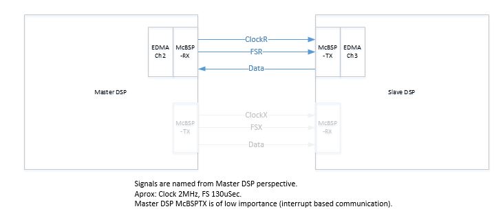
In our board we have 2 DSPs. 

Master DSP is configured to generate Frame sync and clock and receive blocks of data (20 bytes for each FS). McBSP is mapped to EDMA to recieve the data and copy to ping-pong buffers.

Slave DSP is configured to send data over McBSP and is configured to use FS generated by external device.

With above configuration, the communication is fine under normal conditions.

But if we reset Main DSP, it looses the data alignment.

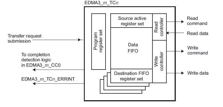
I would like to understand the behavior of EDMa in above situations.

In Slave DSP, how does the EDMA synchronizes its pointers to the Frame sync of Master  when master DSP restarts .

Similar discussion happened in this thread but couldn't get any answer.

e2e.ti.com/.../272109

  • Hi,

    To know the behaviour of EDMA on such situation, there is ping pong buffering EDMA example configuration in which you could understand the synchronization with DSP, kindly refer section 3.4.4 from the c645x EDMA controller user guide as below:

    http://www.ti.com/lit/ug/spru966c/spru966c.pdf

    Kindly comply with the above McBSP ping pong buffering PaRAM configuration and try to understand the EDMA behaviour.

    Thanks & regards,

    Sivaraj K

    ------------------------------------------------------------------------------------------------

    Please click the Verify Answer button on this post if it answers your question.

    ------------------------------------------------------------------------------------------------

  • From section 3.4.4.1 of above document
    "In this example, both channels provide their channel numbers as their report word and set the TCINTEN bit to generate an interrupt after completion. When
    channel 13 fills an input buffer, the E13 bit in the interrupt pending register (IPR) is set; ; when channel 12 empties an output buffer, the E12 bit in IPR is set. "
    My question is, while emptying the output buffer, if external device stops giving clock (due to restart of that device) the output buffer of this device is half empty.
    If the external device start sending clock again (along with a new FS after restart), it expects a new set of data.
    But this device, with half empty output buffer starts sending remaining data.

    I would like to know if there is a way to re-align the EDMA output buffer params (counts) when a Frame sync starts in middle of the buffer count .

    Another question is, with similar configuration, I'm not seeing this alignment issue in 6711 and 6713 processors. I'm seeing this problem with c6746 processors.
  • From above Fig, "Source Active register set" holds the current transaction. 

    My concern is how to flush out the half finished "Source active register set" (its half finished because Master device stopped giving clock due to restart of that device)., And start with a new set when next frame sync arrives from Master device.

    Lets say,

    -McBSP TX is linked with EDMA here for sending out 16 bytes

    -In Source active register set, source address is incremented by 6 bytes and 10 bytes are pending.

    -Master device stopped clock (due to restart).

    - Master device started a new frame sync and started sending clock.

    In this situation, it looks like "Active register set" is sending remaining 10 bytes.

    But I need to discard this half done "Active register set" and start new set of data.

    How to achieve this.

  • As I mentioned in my posts, there is no problem after a power ON of the board (which has two DSPs in master - slave mode).

    No data alignment issues with first power-on.

    Misalignment happens, only when master DSP is hard-reset, while slave DSP is continued running.

    Surprisingly, misalignment is not of random length, it ranges from 1 to 3 bytes.

    For the correct sequence of:

    00 01 02 03 04 05 06 07 08 09 0A 0B 0C 0D 0E 0F,

    It becomes one of below sequence at recieving end of Main DSP:

    0F 00 01 02 03 04 05 06 07 08 09 0A 0B 0C 0D 0E

    or

    0E 0F 00 01 02 03 04 05 06 07 08 09 0A 0B 0C 0D

    or

    0D 0E 0F 00 01 02 03 04 05 06 07 08 09 0A 0B 0C

    I'm not clear if its because EDMA using half finished param set or something else.

    Any suggestions are welcome.

  • Is there any method to clean restart the EDMA module alone?

  • Bhaskar,

    There is not a way to cleanly reset the EDMA3. Restarting it means to program it again, and that depends a lot on what is actively going on (which has to be stopped first).

    You have only given a portion of the system description, since you were looking for a specific reset/restart solution. More information will be needed to come up with a practical solution. Here are some early ideas until we know more:

    1. Do not reset the Master DSP. If you can make it branch to _c_int00 instead of doing a hardware reset, you might be able to maintain synchronization.

    2. Reset both DSPs at the same time. This will allow the normal power-up sequence to get the McBSPs in sync.

    3. Send a signal to the Slave DSP to indicate when the Master DSP has been reset. You could then reset the McBSP on the Slave, and then its EDMA3 channels (since the McBSP would be halted), and let things start up the same as the normal power-up sequence. The signal could be a GPIO signal or even the RESET signal that goes into the Master DSP.

    Some good datapoints to tell us about your configuration are:

    - McBSP configuration: BFIFO depth, bit rate, frame rate, and such.
    - DMA channel configuration: OPT, ACNT, BCNT

    Regards,
    RandyP
  • Hi RandyP,

    Thanks for your inputs.

    We don't have control on Reset. Though the two DSPs are on same board, they have different power supplies sourced independently.

    My concern is with random power cycles on Master DSP.

    If any of the DSP is power-cycled or reset independently, the board should come back normal.

    In your 3rd point, i'm assuming Main DSP has to send signal before it resets which is not possible due to above reasons.

    As FS is programmed to be around 130uSec, EDMA ISRs will be occurring at that rate in both Master and Slave DSP.

    When ISR is stopped, Slave DSP knows that Master DSP is stopped and can re-initialize McBSP and EDMA before Master DSP comes back again.

    But this re-initialization is not clean as there is a pending transaction (previous EDMA transaction /param set is not finished as the clock is stopped abruptly).

    Note that while doing this re-initialization in Slave DSP,

    -Master DSP is not started yet

    -As part of re-init Slave DSP disables McBSP first and enables at the end of init.

    How to flush out that half finished EDMA transaction before Master DSP comes back.

    Connection diagram..

    Init

    #ifdef SLAVE
    Uint8 McbspTxBuffer[2][20];
    #else
    Uint8 MCBSP0RcvBuffer[2][20];
    #endif
    
    
    void InitMcbsp0(void)
    {
    	    MCBSP0_SPCR = 0;
    
    #ifndef SLAVE
    
    		/* Master DSP init */
    
    	    /*Pin Multiplexing for Mcbsp */
    		/*Select function CLKRO ,CLKX0,FSR0,FSX0,DR0 and DX0 */
    		PINMUX2 = 0x02222220;
    
    	    /*Pin control register(Master:Receive data sampled on falling edge of CLKR.
    	     *Transmit data driven on rising edge of CLKX*
    	     *The input clock for the sample rate generator is taken from
    	     *the McBSP internal input clock*
    	     *CLKR is an output pin and is driven by internal clock.*
    	     *CLKX is an output pin and is driven by internal clock.*
    	     *Frame-synchronization signal is generated internally by
    	     *the sample-rate generator. FSR is an output pin.*
    	     *Frame-synchronization signal is determined by FSGM bit in SRGR.*/
    		MCBSP0_PCR = 0x00000f00;
    		/*Receive Control Register : 8 bit Receive , 16 Frame width , 1 bit delay*/
    		MCBSP0_RCR = 0x00010F00;
    		/*Transmit Control Register : 8-bit Trans, No frame width , 1 bit delay */
    		MCBSP0_XCR = 0x00010000;
    		MCBSP0_DXR = 0;
    		/*Multi-channel Control Register :Block 0: channels 0 through 15 */
    		MCBSP0_MCR =0x00000000;
    		/*Enhanced Receive Channel Enable Registers: */
    		MCBSP0_RCERE0 = 0xFFFF;
    		/*Sample rate generator register: divide clock by 75, frame width period 256,
    	    derive sample rate from clock 300M/2/75, The input clock for the sample rate
    	    generator is taken from the McBSP internal input clock*/
    		MCBSP0_SRGR =0x2100004B;
    		/*Serial Port Control Register : Sample-rate generator is taken out of reset*/
    		MCBSP0_SPCR = 0x00400000;
            /* Set Recieve fifo width to 16 Bytes */
    		MCBSP0_RFIFOCTL =  0;
    		/*Serial Port Control Register : Sample rate generator is taken
    		 * out of rest and Frame Sync Generation FPGR+1 in MCBSP0_SRGR*
    		 * Enable continuous clocking to TX and RX Clocking when emulating
    		 * halt also*/
    		MCBSP0_SPCR = 0x03C00000;
    #else
    
    		/*Save DSP init*/
    
    		/*Select function CLKRO ,CLKX0,FSR0,FSX0,DR0 and DX0 */
    		PINMUX2 = 0x02222220;
    		/*For Slave DSP CLKR, CLKX and FS are driven by Main DSP */
    		MCBSP0_PCR = 0x00000000;
            /* Enable System clock for MCbsp */
    		CFGCHIP3 &= ~(1 << 4);
    		/*Receive Control Register : 8 bit Receive , No Frame width , 1 bit delay*/
    		MCBSP0_RCR = 0x00010000;
    
    		/*Transmit Control Register : 8-bit Transfer , 16 frame width , 1 bit delay */
    		MCBSP0_XCR = 0x00050F00;
    
    		MCBSP0_MCR = 0x00000000;
    
    		MCBSP0_XCERE0 = 0xFFFF;
            /* XINT is generated by XSYNC Error */
    		MCBSP0_SPCR = 0x00300000;
    
    		MCBSP0_WFIFOCTL =  0;
    
    #endif
    		/* Initialize EDMA */
    		EdmaInit(MSBSP0_SRC1);
            /* Enable Transmit and Receive */
    		MCBSP0_SPCR |= 0x00010001;
    
    }
    
    
    void EdmaInit()
    {
    #ifndef SLAVE
    
    		/* Master DSP */
    
    		/* EDMA MAIN CHANNEL for Mcbsp transmit main channel */
    		*((unsigned int *) (EVENT2_PARAMS + OPT)) = 0x00000000;
    		*((unsigned int *) (EVENT2_PARAMS + OPT)) = 0x00102000;
    		*((unsigned int *) (EVENT2_PARAMS + SRC)) = 0x01F10000;
    		*((unsigned int *) (EVENT2_PARAMS + CNT)) = 0x00100001;
    		*((unsigned int *) (EVENT2_PARAMS + DST)) = (unsigned int)&MCBSP0RcvBuffer[PING];
    		*((unsigned int *) (EVENT2_PARAMS + IDX)) = 0x00010000;
    		*((unsigned int *) (EVENT2_PARAMS + LNK)) = (REVENT3_PARAMS  & 0xffff);
    		*((unsigned int *) (EVENT2_PARAMS + LNK)) |= 0x00100000;
    		*((unsigned int *) (EVENT2_PARAMS + SRC_DST_CIDX)) = 0x00000000;
    		*((unsigned int *) (EVENT2_PARAMS + CCNT)) = 1;
    
    		/* EDMA RELOAD CHANNEL for Mcbsp transmit (PONG) */
    		*((unsigned int *) (REVENT3_PARAMS + OPT)) = 0x00000000;
    		*((unsigned int *) (REVENT3_PARAMS + OPT)) = 0x00102000;
    		*((unsigned int *) (REVENT3_PARAMS + SRC)) = 0x01F10000;
    		*((unsigned int *) (REVENT3_PARAMS + CNT)) = 0x00100001;
    		*((unsigned int *) (REVENT3_PARAMS + DST)) = (unsigned int)&MCBSP0RcvBuffer[PONG];
    		*((unsigned int *) (REVENT3_PARAMS + IDX)) = 0x00010000;
    		*((unsigned int *) (REVENT3_PARAMS + LNK)) = (REVENT4_PARAMS & 0xffff);
    		*((unsigned int *) (REVENT3_PARAMS + LNK)) |= 0x00100000;
    		*((unsigned int *) (REVENT3_PARAMS + SRC_DST_CIDX)) = 0x00000000;
    		*((unsigned int *) (REVENT3_PARAMS + CCNT)) = 1;
    
    		/* EDMA RELOAD CHANNEL RELOAD for Mcbsp transmit (PING) */
    		*((unsigned int *) (REVENT4_PARAMS + OPT)) = 0x00000000;
    		*((unsigned int *) (REVENT4_PARAMS + OPT)) = 0x00102000;
    		*((unsigned int *) (REVENT4_PARAMS + SRC)) = 0x01F10000;
    		*((unsigned int *) (REVENT4_PARAMS + CNT)) = 0x00100001;
    		*((unsigned int *) (REVENT4_PARAMS + DST)) = (unsigned int)&MCBSP0RcvBuffer[PING];
    		*((unsigned int *) (REVENT4_PARAMS + IDX)) = 0x00010000;
    		*((unsigned int *) (REVENT4_PARAMS + LNK)) = (REVENT3_PARAMS & 0xffff);
    		*((unsigned int *) (REVENT4_PARAMS + LNK)) |= 0x00100000;
    		*((unsigned int *) (REVENT4_PARAMS + SRC_DST_CIDX)) = 0x00000000;
    		*((unsigned int *) (REVENT4_PARAMS + CCNT)) = 1;
    
    		/*The DMA region access enable registers for shadow region 1 */
    		EDMA0_DRAE1 = EDMA_MCBSP0_RX_EVENT;
    		/*Clear the transfer compete interrupt*/
    		EDMA0_SIECR = EDMA_MCBSP0_RX_EVENT;
    		EDMA0_SICR |= EDMA_MCBSP0_RX_EVENT;
    		/*Event 2 is queued on Q0.*/
    		EDMA0_DMAQNUM0 &= ~EDMA_MCBSP0_RX_EVENT;
    		/*Event Enable Set Register for event 2*/
    		EDMA0_SEESR = EDMA_MCBSP0_RX_EVENT;
    		/* Enable the Transfer complete interrupt */
    		EDMA0_SIESR = EDMA_MCBSP0_RX_EVENT;
    
    #else
    
    	/* Slave DSP */
    
    	/* EDMA MAIN CHANNEL for Mcbsp transmit Main channel */
        *((unsigned int *) (EVENT3_PARAMS + OPT)) = 0x00000000;
    	*((unsigned int *) (EVENT3_PARAMS + OPT)) = 0x00103000;
    	*((unsigned int *) (EVENT3_PARAMS + SRC)) = (unsigned int)&McbspTxBuffer[PING];
    	*((unsigned int *) (EVENT3_PARAMS + CNT)) = 0x00100001;
    	*((unsigned int *) (EVENT3_PARAMS + DST)) = 0x01F10000 ;
    	*((unsigned int *) (EVENT3_PARAMS + IDX)) = 0x00000001;
    	*((unsigned int *) (EVENT3_PARAMS + LNK)) =  (REVENT3_PARAMS & 0xffff);
    	*((unsigned int *) (EVENT3_PARAMS + LNK)) |= 0x00100000;
    	*((unsigned int *) (EVENT3_PARAMS + SRC_DST_CIDX)) = 0x00000001;
    	*((unsigned int *) (EVENT3_PARAMS + CCNT)) =1;
    
    	/* EDMA RELOAD CHANNEL for Mcbsp transmit (PONG) */
    	*((unsigned int *) (REVENT3_PARAMS + OPT)) = 0x00000000;
    	*((unsigned int *) (REVENT3_PARAMS + OPT)) = 0x00103000;
    	*((unsigned int *) (REVENT3_PARAMS + SRC)) = (unsigned int) &McbspTxBuffer[PONG];
    	*((unsigned int *) (REVENT3_PARAMS + CNT)) = 0x00100001;;
    	*((unsigned int *) (REVENT3_PARAMS + DST)) = 0x01F10000;
    	*((unsigned int *) (REVENT3_PARAMS + IDX)) = 0x00000001;
    	*((unsigned int *) (REVENT3_PARAMS + LNK)) = (REVENT4_PARAMS & 0xffff);
    	*((unsigned int *) (REVENT3_PARAMS + LNK))|= 0x00100000;
    	*((unsigned int *) (REVENT3_PARAMS + SRC_DST_CIDX)) = 0x00000001;
    	*((unsigned int *) (REVENT3_PARAMS + CCNT)) = 1;
    
    	/* EDMA RELOAD CHANNEL RELOAD for Mcbsp transmit (PING) */
    	*((unsigned int *) (REVENT4_PARAMS + OPT)) = 0x00000000;
    	*((unsigned int *) (REVENT4_PARAMS + OPT)) = 0x00103000;
    	*((unsigned int *) (REVENT4_PARAMS + SRC)) = (unsigned int) &McbspTxBuffer[PING];
    	*((unsigned int *) (REVENT4_PARAMS + CNT)) = 0x00100001;
    	*((unsigned int *) (REVENT4_PARAMS + DST)) = 0x01F10000;
    	*((unsigned int *) (REVENT4_PARAMS + IDX)) = 0x00000001;
    	*((unsigned int *) (REVENT4_PARAMS + LNK)) = (REVENT3_PARAMS & 0xffff);
    	*((unsigned int *) (REVENT4_PARAMS + LNK))|= 0x00100000;
    	*((unsigned int *) (REVENT4_PARAMS + SRC_DST_CIDX)) = 0x00000001;
    	*((unsigned int *) (REVENT4_PARAMS + CCNT)) = 1;
    
     	/*The DMA region access enable registers for shadow region 1 */
    	EDMA0_DRAE1 = EDMA_MCBSP0_TX_EVENT;
        /*Clear the transfer complete interrupt*/
    	EDMA0_SIECR = EDMA_MCBSP0_TX_EVENT;
    	/*Event 3 is queued on Q0.*/
    	EDMA0_DMAQNUM0 &= ~EDMA_MCBSP0_TX_EVENT;
    	/*Event Enable Set Register for event 3*/
    	EDMA0_SEESR = EDMA_MCBSP0_TX_EVENT;
    	/* Enable the Transfer complete interrupt */
    	EDMA0_SIESR = EDMA_MCBSP0_TX_EVENT;
    
    #endif
    }
    
    
    Code attached.

    But with same configuration, this kind of issue was not observed on 6711 and 6713 platform. 

  • Hi,

    Please evaluate the cause which blocks the pending EDMA transaction to complete. How is the DMA PaRAM set configured for the mapped DMA channel to peripheral triggered event and kindly validate this?

    Is your TR programmed for normal completion or early completion? Did you configured EDMA for chain triggered transfer? Usually the TR packets from EDMA CC would be queued in the TC and would be serviced based on priority mechanism

    In case, if TR is programmed for early completion, it should be quite normal since the transfer is considered to be complete after the EDMACC submits a TR to the EDMATC but the TC may still be transferring the data and in this mode, the channel controller would generate the TCC internally which indicates the transfer is said to be complete but the actual transfer would be still in progress. Please think about all possible usecase scenario.

    Alternatively, you could also think of the queue priority mechanism of TC's TR packets as well data traffic and due to which, you could also experience the latency of DMA data transfer to the destination.

    The above are my early i deas but it should be finely tuned to narrow down the root cause.

    Thanks & regards,

    Sivaraj K

    ------------------------------------------------------------------------------------------------------

    Please click the Verify Answer button on this post if it answers your question.

    -------------------------------------------------------------------------------------------------------

  • Though my post mentioned reasons, i'm re-posting again.

    Sivaraj Kuppuraj said:

    Please evaluate the cause which blocks the pending EDMA transaction to complete. How is the DMA PaRAM set configured for the mapped DMA channel to peripheral triggered event and kindly validate this?

    Because external clock is stopped for the McBSP which is configured to use the external clock for TX.

    Sivaraj Kuppuraj said:

    Is your TR programmed for normal completion or early completion? Did you configured EDMA for chain triggered transfer? Usually the TR packets from EDMA CC would be queued in the TC and would be serviced based on priority mechanism

    In case, if TR is programmed for early completion, it should be quite normal since the transfer is considered to be complete after the EDMACC submits a TR to the EDMATC but the TC may still be transferring the data and in this mode, the channel controller would generate the TCC internally which indicates the transfer is said to be complete but the actual transfer would be still in progress. Please think about all possible usecase scenario.

    I have already attached McBSP and EDMA init code.

    Sivaraj Kuppuraj said:

    Alternatively, you could also think of the queue priority mechanism of TC's TR packets as well data traffic and due to which, you could also experience the latency of DMA data transfer to the destination.

    I'm not sure how that helps.

    As mentioned in this thread,

    I'm looking for work around to clear the half finished EDMA param set and start with a new set when next frame sync arrives.

  • Bhaskar,

    You will get better performance from your EDMA if you use the BFIFO in the McBSP. If your data rate is very high, the EDMA3 will be kept pretty busy servicing individual bytes. If your data rate is low enough or your other use of the EDMA3 is minimal, then it will not matter.

    There are a lot of possible race conditions that can make re-syncing difficult. Your situation is not completely clear, yet.

    If the Slave DSP is able to detect that the Master DSP has stopped sending, then the Slave McBSP needs to be stopped to prepare for re-syncing and the EDMA3 needs to be re-initialized for the few channels that are being used by the Slave McBSP port.

    1. Stop the Slave McBSP so it cannot generate any new events to the EDMA3.
    2. Disable the McBSP events in the EDMA3 EER.
    3. Reprogram the active PARAM set so it will be ready for the first new event from the McBSP.
    4. Make sure the SER and EMR registers are cleared for the McBSP DMA channels.
    5. Follow the guidelines in the McBSP User Guide to get the McBSP and EDMA3 ready for operation, which will include setting the EER bit and restarting the McBSP.

    Your C code does not reference a header file and there are registers listed that do not match any of the TI documents that I could find, such as EDMA0_SEESR and EDMA0_SIESR. It will help in the future for you to use register names we can recognize from the TI header files and/or TI documentation. It may not matter here, but I cannot tell if you are setting up the interrupts correctly; I will assume you are since that is not part of your thread.

    Depending on the time you have available with no McBSP clock, you might be able to do the re-sync by just copying one of the LINK PARAM sets to the channel's PARAM set. If nothing else is happening during that time, that could do it all for you.

    Regards,
    RandyP

  • Thank you for your support.

    RandyP said:


    Depending on the time you have available with no McBSP clock, you might be able to do the re-sync by just copying one of the LINK PARAM sets to the channel's PARAM set. If nothing else is happening during that time, that could do it all for you.

    We have introduced intentional delay in Master DSP startup (so that, if it resets, it waits enough time before it starts sending McBSP clock).

    Copying of Link PARAMs to channel params has no affect.

    I kept the Main DSP in reset state and viewed EDMA registers of Slave DSP in debug mode. As there is no clock coming in, no further events can happen in Slave DSP.

    After re-initializing EDMA in slave DSP, I observed that the Register SASRC (Source Active Source Address Register) is holding some intermediate pointer (buffer pointer where it halted ) instead of  the starting address of my TX buffer loaded in Param registers. This address is same as the one before re-initialization. None of the bits in SER register are set.

    When the Main DSP releases the clock, it looks like it is resuming from the pointer where it is halted.

    I tried another workaround which seems to be working:

    After Slave DSP detected loss of comm,

    • set a flag to indicate there is a comm fail.
    • In the EDMA ISR check if above flag is set, if set then immediately disable the clock. (this ISR occurs after Master DSP resumes clock). And then re-initialize the param set.

    But my expectation is, Re-initialization EDMA done before the Master DSP resumes clock also work.

  • Bhaskar,

    Bhaskar Reddy said:
    Copying of Link PARAMs to channel params has no affect.

    I am not sure what this means. Before copying, the channel PARAM set should have a source address incremented by 1 from what is in the SASRC, so changing it back to the correct starting address should make the results different. Since you have a solution, it probably does not matter whether I understand or not.

    Bhaskar Reddy said:
    After re-initializing EDMA in slave DSP, I observed that the Register SASRC (Source Active Source Address Register) is holding some intermediate pointer (buffer pointer where it halted ) instead of  the starting address of my TX buffer loaded in Param registers. This address is same as the one before re-initialization.

    What you observe in SASRC is correct. It will always show what it most recently did based on the last Transfer Request. When the last TR came in, it was for a single byte transfer and its source address will be placed in SASRC. When the source active register set completes its reading of data from the source address. It is appropriate that when you look at SASRC you see the last address read.

    Bhaskar Reddy said:
    When the Main DSP releases the clock, it looks like it is resuming from the pointer where it is halted.

    The Slave DSP should resume from whatever has been programmed into the Channel's PARAM, meaning EVENT3_PARAMS.

    Bhaskar Reddy posted code said:
         /*The DMA region access enable registers for shadow region 1 */
        EDMA0_DRAE1 = EDMA_MCBSP0_TX_EVENT;
        /*Clear the transfer complete interrupt*/
        EDMA0_SIECR = EDMA_MCBSP0_TX_EVENT;
        /*Event 3 is queued on Q0.*/
        EDMA0_DMAQNUM0 &= ~EDMA_MCBSP0_TX_EVENT;
        /*Event Enable Set Register for event 3*/
        EDMA0_SEESR = EDMA_MCBSP0_TX_EVENT;
        /* Enable the Transfer complete interrupt */
        EDMA0_SIESR = EDMA_MCBSP0_TX_EVENT;

    The EDMA_MCBSP0_TX_EVENT constant is usually an event number, 0-63, but you are using it as a bit mask. In any case, the DMAQNUM0 assignment does appear to do what the comment suggests is intended; That assignment could be removed or modified depending on your requirements.

    Bhaskar Reddy said:
    In the EDMA ISR check if above flag is set, if set then immediately disable the clock. (this ISR occurs after Master DSP resumes clock). And then re-initialize the param set.

    If this is an acceptable work-around, then we can close this thread by you marking your work-around post with Verify Answer. Or we can continue the discussion if you want to.

    Regards,
    RandyP