Hello,
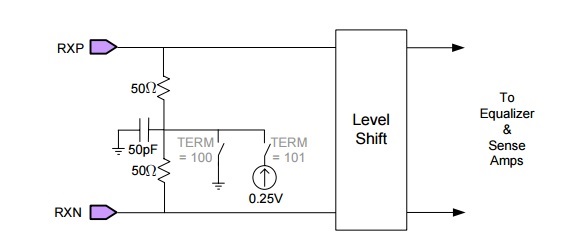
One of my customer is asking whether or not block diagram is available for PCIe internal logic, especially, termination logic for data line.
Here is the schematic review checklist :
And it suggests external termination is not required to data lines. So now they are interested in the block diagram of PCIe internal logic to confirm it looks like the following:
This snapshot is from the device connected to C6655 via PCIe.
Can you share such information here ?
Best Regards,
Naoki Kawada


