


Hello. We have created a board based on the 66AK2E05 SoC and cannot find a way to boot up using a GPH image in NOR Flash and read via SPI. The board powers up and remains stuck in an RBL loop. The BOOTCOMPLETE register is never updated, but the binary image from NOR Flash is properly downloaded to the start of SRAM (0x0c000000), just never executed.
Using a JTAG probe with CCS the DEVSTAT register was shown to contain what we had configured via the input pins to the chip:
DEVSTAT = 0x00009005
Boot Mode Pins
--------------
16 15 14 13 12 11 10 9 8 7 6 5 4 3 2 1
--- --- --- --- --- --- --- --- --- --- --- --- --- --- --- ---
0 1 0 0 1 0 0 0 0 0 0 0 0 0 1 0
Width | Csel | Mode | Port | ARM | Param Idx | Min | SPI |
24-bit adr| 1 | 0 | SPI0 | | ParamTable[0] |full |
The boot parameter tables at 0x0c1b0500 for core 0 are:
Addr\Ofst: 0 1 2 3 4 5 6 7 8 9 A B C D E F
---------- -- -- -- -- -- -- -- -- -- -- -- -- -- -- -- --
0x0c1B0500 2E 00 00 00 32 00 00 00 00 00 00 00 00 00 00 00
0x0c1B0510 38 01 38 01 01 00 03 00 18 00 08 00 FE FF 02 00
0x0c1B0520 01 00 05 00 00 00 00 00 00 00 00 00 00 00 00 00
0x0c1B0530 00 00 00 00 00 00 00 00 00 00 00 00 00 00 00 00
0x0c1B0540 00 00 00 00 00 00 00 00 00 00 00 00 00 00 00 00
0x0c1B0550 00 00 00 00 00 00 00 00 00 00 00 00 00 00 00 00
0x0c1B0560 00 00 00 00 00 00 00 00 00 00 00 00 00 00 00 00
0x0c1B0570 00 00 00 00 00 00 00 00 00 00 00 00 00 00 00 00
0x0c1B0580 18 00 00 00 64 00 00 00 00 00 00 00 00 00 00 00
0x0c1B0590 38 01 38 01 00 00 00 00 00 00 00 00 00 00 00 00
0x0c1B05A0 00 00 00 00 00 00 00 00 00 00 00 00 00 00 00 00
0x0c1B05B0 00 00 00 00 00 00 00 00 00 00 00 00 00 00 00 00
0x0c1B05C0 00 00 00 00 00 00 00 00 00 00 00 00 00 00 00 00
0x0c1B05D0 00 00 00 00 00 00 00 00 00 00 00 00 00 00 00 00
0x0c1B05E0 00 00 00 00 00 00 00 00 00 00 00 00 00 00 00 00
0x0c1B05F0 00 00 00 00 00 00 00 00 00 00 00 00 00 00 00 00
We are not certain if this RBL generated table is correct. The fact that the binary image is properly downloaded to SRAM from NOR Flash via SPI seems to validate it. However, inspection of byte 20 (0x14) indicates a C66x DSP boot mode. The 66AK2E05 data sheet states explicitly that C66x DSP boot modes are NOT supported. This seems to borne out by the observation that ARM core 0 is executing the RBL.
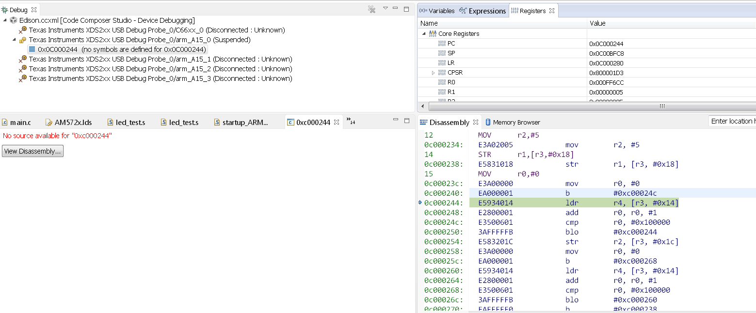
The binary image is super simple, merely setting up and twiddling a couple of GPIO bits attached to LEDs in a continuous loop:
bootLEDtest:
0030cf80 e3a03cbf MOV r3,#0xbf00
0030cf84 e3403260 MOVT r3, 608 (0x260)
0030cf88 e5930010 LDR r0,[r3,#0x10]
0030cf8c e3c00005 BIC r0,r0,#5
0030cf90 e5830010 STR r0,[r3,#0x10]
0030cf94 e5930014 LDR r0,[r3,#0x14]
0030cf98 e3801005 ORR r1,r0,#5
0030cf9c e3a02005 MOV r2,#5
0030cfa0 e5831018 STR r1,[r3,#0x18]
0030cfa4 e3a00000 MOV r0,#0
0030cfa8 ea000001 B 0x0030cfb4
0030cfac e5934014 LDR r4,[r3,#0x14]
0030cfb0 e2800001 ADD r0,r0,#1
0030cfb4 e3500601 CMP r0,#0x100000
0030cfb8 3afffffb BCC 0x0030cfac
0030cfbc e583201c STR r2,[r3,#0x1c]
0030cfc0 e3a00000 MOV r0,#0
0030cfc4 ea000001 B 0x0030cfd0
0030cfc8 e5934014 LDR r4,[r3,#0x14]
0030cfcc e2800001 ADD r0,r0,#1
0030cfd0 e3500601 CMP r0,#0x100000
0030cfd4 3afffffb BCC 0x0030cfc8
0030cfd8 eafffff0 B 0x0030cfa0
The GPH image looks like this:
00000000: 00000070 0C000000 E3A03CBF E3403260
00000010: E5930010 E3C00005 E5830010 E5930014
00000020: E3801005 E3A02005 E5831018 E3A00000
00000030: EA000001 E5934014 E2800001 E3500601
00000040: 3AFFFFFB E583201C E3A00000 EA000001
00000050: E5934014 E2800001 E3500601 3AFFFFFB
00000060: EAFFFFF0 00000000 00000000 00000000
The RBL documentation is incomplete at best. It never states that the General Purpose Header (GPH) format for blocks is not a standard format. The data payload in a block is little endian for direct execution by core 0, but the two-word head MUST BE BIG ENDIAN. That is obvious in the above.
Note that the binary code is assembled using the Gnu ARM assembler supplied with our Wind River Systems Workbench 4.0 IDE. We are not using CCS or MCSDK to develop our boot code, but could switch to using it if we can get the JTAG probe to work with CCS using no .gel file. (The only way to be certain the boot code is complete and can stand alone.
The power up sequence is not ideal. CCS will not allow us to put the target connection attempt in an automatic retry sequence, so we must first power up the board then tell CCS to connect to the board. By that time, core 0 is already in the RBL loop, but the Power On Reset (POR) state is still active so we can see what memory has in it. We have no RBL source code, so trying to trace the RBL loop is meaningless – we do not want to reverse engineer RBL. Consequently, we cannot determine why RBL is failing to execute the binary boot code in SRAM.
Has anyone seen this problem before or have any suggestions to work around it?
Thanks in advance for any assistance.
Mitch


