


Hi TI expert,
In 6670 EVM from Advantech,
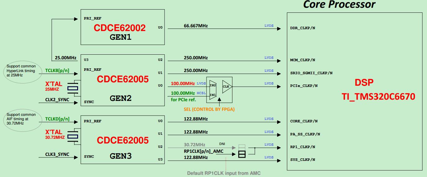
I see the GEN3 uses 30.72Mhz XTAL to generate 122.88MHz as CORE_CLK, 122.88MHz as PASS_CLK, 30.72MHz as RP1_CLK and 122.88MHz as SYSCLK.
And GEN2 uses 25MHz XTAL to generate 250MHz as MCMCLK, 250MHz as SRIOSGMIICLK, 100MHz as PCIECLK and 25MHz as refclk to CDCE62002.
Then CDCE62002 generates 66.67MHz as DDR3 controller clock input using 25MHz from GEN2 as reference.
In my project, I delete the CDCE62002 and use GEN2 to generate 83.33MHz. And I use this 83.33MHz as DDR3 controller clock input.
The GEN2 CDCE62005's configuration is below


At this time, the PCB layout is in progress.
And I must confirm that when the DDR3 controller's clock input is 83.33MHz and set PLLM_DDR to 31 and PLLD_DDR to 1, the C6670's DDR3 PLL can generate 83.33MHz*(31+1)/(1+1)=1333.28MHz. And this configuration can run DDR3 DRAM correctlly.
1. Please help me to confirm if it is OK.
2. If DDR3 does not run normal clock like 800MHz, 1066MHz and 1333MHz but run at 1210MHz for example, will the DDR3 go unstable?
It is very urgent to me, because the PCB layouting is already in progress.
Thanks!
Feng
