This thread has been locked.

If you have a related question, please click the "Ask a related question" button in the top right corner. The newly created question will be automatically linked to this question.

NOR Direct boot OMAP L 137

Other Parts Discussed in Thread: OMAP-L137

Hi,

I have the following settings and I would like to understand how to boot directly from NOR

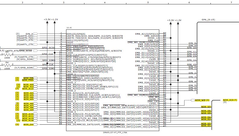
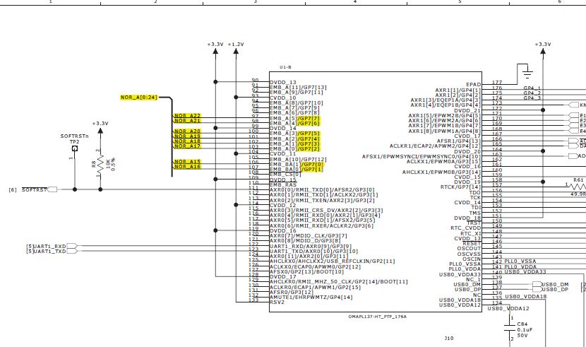
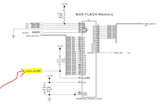
  • I access an external NOR flash (8MB) using EMIFA and GPIO's 
  • My code exceeds 32KB which is the max boot image seen by bootloader in the case of CS2 having 15 address lines EMA_BA[1:0] and EMA_A[12:0]
  • I already used AIS and NORWRITER to flash a small code and it works ok

My question is :

I want to use the method NOR direct described by bootloader document but I don't know how.

I tried to follow the  Talk:Secondary Bootloaders on OMAP-L1x but the .text section is too small for my case.

how can I place all my code in this section knowing that only 32 KB is possible. should I extend the section PROG_NOR to include all the space available in my NOR flash space, and how and where exactly GPIO's would be set to allow CPU reading/writing from/to the upper address lines of the NOR.

MEMORY {

   CFG_NOR:      o = 0x60000000  l = 0x00000020
   PROG_NOR:     o = 0x60000020  l = 0x00003FE0
   PROG_L2RAM:   o = 0x11800000  l = 0x00002000

}

SECTIONS {

   .entryPoint > PROG_NOR
   .text	> PROG_NOR
   .const	> PROG_NOR
   .switch	> PROG_NOR
   .cinit	> PROG_NOR
   
   .far	> PROG_L2RAM
   .data	> PROG_L2RAM
   .bss	> PROG_L2RAM
   .cio	> PROG_L2RAM
   .stack	> PROG_L2RAM
   .sysmem	> PROG_L2RAM
   .nor_cfg_word > CFG_NOR

}


Thank you for your support

  • Hi Ahmed,

    I have experimented writing an image file to NOR memory ( S29AL032D90TFI000 )from spansion of size 32 Mb interfaced with the daughter card board of OMAPL137 SDI board.

    Using NOR writer program ( of OMAP-L137_FlashAndBootUtils_2_43) , able to flash an image of more than 32 KB ( i.e., 37630 bytes) ; which means able to (read and write) access the NOR memory beyond 32KB.

    And also tested flashing files of sizes greater than 64KB and 1MB.

    Send your image file. Let me flash and check whether flashing is successful.

    Please refer to the below screenshots.

  • Hi Shankari,

    Thank you for the support.

    no doubt for an EVM board that would work I think, but in my case I have a custom board so I might need to modify the NORWriter to access the NOR flash beyond the 32 KB seen by the EMIFA and toggle GPIO's that manage the upper address lines.

    in your case how NORwriter controls upper address lines, are you using a spansion driver. 

    I will try NORwriter with big size image and let you know how it goes, but I want to try the method of NOR direct boot mode.

    Thnaks 

    AHmed 

  • Hi Ahmed,

    There are two recommendations here.

    1. Hardware:

    You may have to first look into the schematics of OMAPL137 SDI and its Daughter card board and understand the interfacing of NOR flash through EMIFA. Compare it with your custom board design. As the OMAPL137 processor can be interfaced with NOR of size more than 32KB... that is here in this case it is 32Mb and not 32 KB, you should also be able to interface and access NOR beyond 32KB..No need to toggle the GPIOs for asserting the address lines.

    2. Software :

    Download the NOR writer code which is part of "OMAP-L137_FlashAndBootUtils_2_43" and have a look at the NOR flash initialization code with respect to its flash size and other parameters like Bus width etc. understand the flow how a 32MB NOR flash is initialized and accessed. Check how to modify it for the NOR device which you use.

  • Hi Ahmed,

    Do a walk through on the NOR writer something like below....

    Software :- With respect to the flash size....

    In Nor writer program, have a look at the NOR command sets used below through which they fetch the NOR info and get it filled in the structure . You can print and see the flash size.

    //nor.c
    
    AMD_SoftReset(hNorInfo);
    
    Intel_SoftReset(hNorInfo);
    
    //nor.h
    
    typedef struct _NOR_INFO_
    
    {
    
     ASYNC_MEM_InfoHandle hAsyncMemInfo;
    
     Uint32      flashBase;                    // 32-bit address of flash start
    
     Uint8       busWidth;                     // 8-bit or 16-bit bus width
    
     Uint8       chipOperatingWidth;           // The operating width of each chip
    
     Uint8       maxTotalWidth;                // Maximum extent of width of all chips combined - determines offset shifts
    
     Uint32      flashSize;                    // Size of NOR flash regions in bytes (numberDevices * size of one device)
    
     Uint32      bufferSize;                   // Size of write buffer
    
     NOR_CmdSet  commandSet;                   // command set id (see CFI documentation)
    
     Uint8       numberDevices;                // Number of deives used in parallel
    
     Uint8       numberRegions;                // Number of regions of contiguous regions of same block size
    
     Uint32      numberBlocks[CFI_MAXREGIONS]; // Number of blocks in a region
    
     Uint32      blockSize[CFI_MAXREGIONS];    // Size of the blocks in a region
    
     NOR_ManfID  manfID;                       // Manufacturer's ID
    
     Uint16      devID1;                       // Device ID
    
     Uint16      devID2;                       // Used for AMD 3-byte ID devices
    
     struct _NOR_FXNS_     *hNorFxns;          // Pointer to NOR Function Structure
    
    }

    For memory initialization : //Device.c

    Uint32 DEVICE_ExternalMemInit(Uint32 sdcr, Uint32 sdtimr1, Uint32 sdtimr2, Uint32 sdrcr, Bool use45Div)
    {
      DEVICE_pinmuxControl(0,0xFFFFFF00,0x11111100);  // nEMB_WE, nEMB_RAS, nEMB_CAS, nEMB_CS[0], EMB_CLK, EMB_SDCKE
      DEVICE_pinmuxControl(1,0xFFFFFFFF,0x11111111);  // EMB_A[5], EMB_A[4], EMB_A[3], EMB_A[2], EMB_A[1], EMB_A[0], EMB_BA[0], EMB_BA[1]
      DEVICE_pinmuxControl(2,0x0FFFFFFF,0x01111111);  // EMB_A[12], EMB_A[11], EMB_A[10], EMB_A[9], EMB_A[8], EMB_A[7], EMB_A[6]
      DEVICE_pinmuxControl(5,0xFFFFFFF0,0x11111110);  // EMB_D[6], EMB_D[5], EMB_D[4], EMB_D[3], EMB_D[2], EMB_D[1], EMB_D[0]
      DEVICE_pinmuxControl(6,0xFFFFFFFF,0x11111111);  // EMB_D[14], EMB_D[13], EMB_D[12], EMB_D[11], EMB_D[10], EMB_D[9], EMB_D[8], EMB_D[7]
      DEVICE_pinmuxControl(7,0x00000FFF,0x00000111);  // nEMB_WE_DQM[0], nEMB_WE_DQM[1], EMB_D[15]
    
      if (((sdcr & DEVICE_SDCR_NM_MASK) >> DEVICE_SDCR_NM_SHIFT) == 0x0)
      {
        DEVICE_pinmuxControl(2,0xF0000000,0x10000000);  // EMB_D[31]
        DEVICE_pinmuxControl(3,0xFFFFFFFF,0x11111111);  // EMB_D[23], EMB_D[24], EMB_D[25], EMB_D[26], EMB_D[27], EMB_D[28], EMB_D[29], EMB_D[30]
        DEVICE_pinmuxControl(4,0xFFFFFFFF,0x11111111);  // nEMB_WE_DQM[3], EMB_D[16], EMB_D[17], EMB_D[18], EMB_D[19], EMB_D[20], EMB_D[21], EMB_D[22]
        DEVICE_pinmuxControl(5,0x0000000F,0x00000001);  // nEMB_WE_DQM[2]
      }
    
      // Power ON
      DEVICE_LPSCTransition(PSCNUM1, LPSC_EMIFB, PD0, PSC_ENABLE);
    
      // Configure
      EMIF3C->SDCR    = sdcr;
      EMIF3C->SDTIMR  = sdtimr1;
      EMIF3C->SDTIMR2 = sdtimr2;
      EMIF3C->SDRCR   = sdrcr;
      
      if (use45Div)
      {
        SYSTEM->CFGCHIP[3] = SYSTEM->CFGCHIP[3] | 0x5;
      }
      
      return E_PASS;
    }

  • Thank you Shankari for your assistance,

    I got this picture from the OMAP137 schematic board :

    For my understanding, are these pins {A2 : A8} and {A15 : A21} ( upper address lines) on the NOR flash using the same pins sources from the EMIFA interface. Can you please clarify.

    Thanks for the support 

  • Hi Ahmed,

    Let me loop in hardware engineers to clarify your questions.

    -------------------------
  • Hi Ahmed,

    I guess so, we are almost close to the problem why beyond 32KB, it is not accessible.

    In the schematics of OMAPL137 Daughter card, "EMIFA_CS3n" seems to play a vital role in accessing the upper Address lines from A15 to A21.

    By tweaking the PINmuxing, your issue of accessing beyond 32 KB can be simulated.
    Experimented in the software that if CS3 is not configured in the PIN Muxing, not able to access beyond 32 KB. so, thus this clarifies that the CS3 plays a major role in accessing greater than 32KB.

    In OMAPL137, CS3 is connected and configured correctly, that's why it works beyond 32KBand able to access > 32KB.


    So , adhere to the schematic design of OMAPL137 Daughter card schematic or share your schematics.

  • Ahmed,

    The OMAPL137 EMIFA controller has A[12:0] address lines only. When there is a requirement to use more address lines you may need to use GPIOs as given in figure 5-12 in OMAPL137 device data manual. But in user interface board their implementation is in a different way, they used lower address lines and different chip select to access higher order address in NOR flash.

    Hope it clarifies.

    Regards,
    Senthil
  • Hi Shankari,

    here is my schematic 

    as you see in the schematic I have the last 8 address pin of the NOR flash controlled by GPIO's {GP7P0 to GP7P7} and I have included this highlighted lines inside the NORwriter project (nor.c) to be able to access upper address when we need to.

    // Get info on block address and sizes
    Uint32 NOR_getBlockInfo(NOR_InfoHandle hNorInfo, Uint32 address, Uint32* blockSize, Uint32* blockAddr)
    {
    Int32 i;
    Uint32 currRegionAddr, nextRegionAddr;
    Uint32 GPIOADDR;

    currRegionAddr = (Uint32) hNorInfo->flashBase;
    if ((address < currRegionAddr) || (address >= (currRegionAddr+hNorInfo->flashSize)))
    {
    return E_FAIL;
    }

    for(i=0; i< (hNorInfo->numberRegions); i++)
    {
    nextRegionAddr = currRegionAddr + (hNorInfo->blockSize[i] * hNorInfo->numberBlocks[i]);
    if ( (currRegionAddr <= address) && (nextRegionAddr > address) )
    {
    *blockSize = hNorInfo->blockSize[i];
    *blockAddr = address & (~((*blockSize) - 1));

    //AS added to control upper address external NOR flash

    GPIOADDR = *blockAddr;

    if( GPIOADDR > 0x60007FFF)
    {
    GpioAddress(GPIOADDR);       //toggle gpio's to access specific address 
    }

    break;
    }
    currRegionAddr = nextRegionAddr;
    }
    return E_PASS;
    }

    but the issue is I am still having issues writing after 0x60008000. is this the right approach or I need to place my code in a different function. please clarify 

    Thank you for your support 

    Ahmed

    Regards,

  • Hi Ahmed,
    We have discussed and closed the problem in the below E2E post.
    e2e.ti.com/.../474804