Because of the holidays, TI E2E™ design support forum responses will be delayed from Dec. 25 through Jan. 2. Thank you for your patience.

This thread has been locked.

If you have a related question, please click the "Ask a related question" button in the top right corner. The newly created question will be automatically linked to this question.

DM8148. difference between 2 documents that describes C674x megamodule

Other Parts Discussed in Thread: TMS320DM8148

Hello TI' teams,

I found little difference between 2 documents that describes C67x megamodule on DM8148 processor.

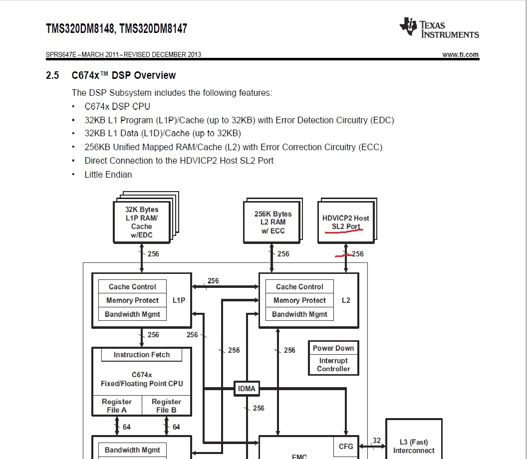
tms320dm8148.pdf describe DSP and megamodule subsystem as:

The DSP Subsystem includes the following features:

• C674x DSP CPU

• 32KB L1 Program (L1P)/Cache (up to 32KB) with Error Detection Circuitry (EDC)

• 32KB L1 Data (L1D)/Cache (up to 32KB)

• 256KB Unified Mapped RAM/Cache (L2) with Error Correction Circuitry (ECC)

• Direct Connection to the HDVICP2 Host SL2 Port

• Little Endian


When DM8148 TRM (sprugz8e.pdf and sprufk5a.pdf) :

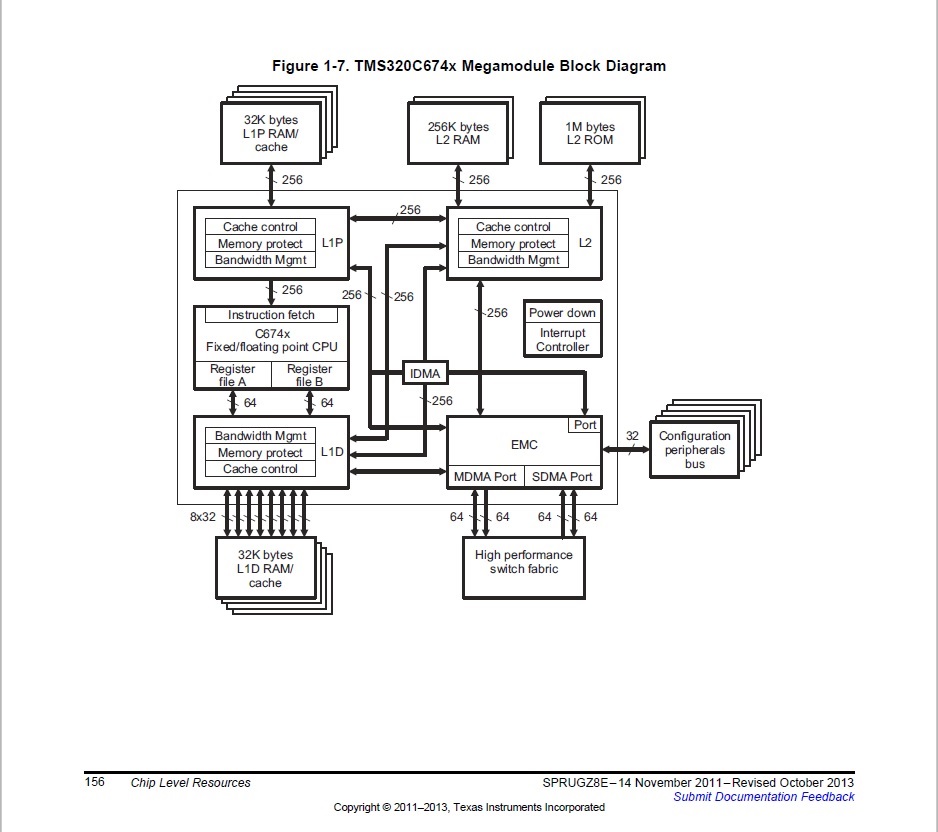
The C674x megamodule (Figure 1-7) consists of the following components:

• TMS320C674x CPU

• Internal memory controllers:

– Level 1 program memory controller (PMC)

– Level 1 data memory controller (DMC)

– Level 2 unified memory controller (UMC)

– Extended memory controller (EMC)

– Internal direct memory access (IDMA) controller

• Internal peripherals:

– Interrupt controller (INTC)

– Power-down controller (PDC)

– Bandwidth manager (BWM)

• Advanced event triggering (AET)...

And no any word about connect between c674x/L2 to HDVICP2.


C674x megamodule block diagram different too in TRM and in tms320DM8148.pdf - plz see attcahed images.

The difference: 256 bits bus "Direct Connection to the HDVICP2 Host SL2 Port".

Please let me known, what diagram is wrong?

  • Hi Marat,

    DM814x datasheet is the correct one. You can also see the connection between C674x DSP and HDVICP2 SL2 in DM814x TRM 1.8.3.2 HDVICP2 IPC

    BR
    Pavel
  • Hi Pavel,
    ThanX a lot for your reply.
    Am I understood correctly (please confirm), that c674x L2 controller has 6 buses are as following:
    256 bits bidirectional bus to L2RAM
    256 bits bidirectional bus to L1P
    256 bits bidirectional bus to L1D
    256 bits bidirectional bus to IDMA engine
    256 bits bidirectional bus to EMC
    and 256 bits bidirectional bus to HDVICP2 SL2 port.

    Am I understood correctly, that 256K of L2/SRAM from C674x megamodule and 256K Shared L2 from HDVICP (SL2) these are differents cache/RAM modules, or L2/SRAM 256K from megamodule shared with HDVICP2?

    And last question please: each transfer initiator inside of megamodule (besides of L1P) has a registers for bandwidht management, please see "SPRUFK5A.pdf" page 146: Table 6-2. Arbitration Registers.

    Please let me known - what kind of register used for bandwidth management of HDVICP/SL2 initiator (if exist)?
    BR
    Marat
  • Marat,

    Marat Shchuchinsky said:
    Am I understood correctly (please confirm), that c674x L2 controller has 6 buses are as following:
    256 bits bidirectional bus to L2RAM
    256 bits bidirectional bus to L1P
    256 bits bidirectional bus to L1D
    256 bits bidirectional bus to IDMA engine
    256 bits bidirectional bus to EMC
    and 256 bits bidirectional bus to HDVICP2 SL2 port.

    Yes, I see exactly this in the datasheet

    Marat Shchuchinsky said:
    Am I understood correctly, that 256K of L2/SRAM from C674x megamodule and 256K Shared L2 from HDVICP (SL2) these are differents cache/RAM modules, or L2/SRAM 256K from megamodule shared with HDVICP2?

    These are different 256KB memories. See datasheet, section 2.12.2 C674x Memory Map

    Marat Shchuchinsky said:
    And last question please: each transfer initiator inside of megamodule (besides of L1P) has a registers for bandwidht management, please see "SPRUFK5A.pdf" page 146: Table 6-2. Arbitration Registers.

    Please let me known - what kind of register used for bandwidth management of HDVICP/SL2 initiator (if exist)?

    See if the below two documents will help:


    3617.DM814x_DM810x_Performance.pdf

    DM8168_Performance.ppt

    BR
    Pavel

  • Thanks a lot again.

    And last please - what is L2 controller / L2RAM clock rate and IDMA0/1 clock rate?

    Is the clock rate equal to C674x CPU clock rate?

  • Marat,

    I think IDMA clock rate is same as C674x CPU clock rate, I can not find any SW configurable or fixed clock divider/multiplier to change the clock that is input to the C674x DSP module to the IDMA. What I found is that EMC (Extended Memory Controller) clock is half the C674x CPU clock, see C674x DSP megamodule reference guide (sprufk5a.pdf).

    Regarding L2 cache, I found that it is clocked at CPU/2, see C674x DSP Cache User's Guide (SPRUG82A), section 1.4 Why Use Cache

    When C674x CPU clock is 600MHz, L1 cache is 600MHz, L2 cache is 300 MHz.

    BR
    Pavel