This thread has been locked.

If you have a related question, please click the "Ask a related question" button in the top right corner. The newly created question will be automatically linked to this question.

Question about DSP's DDR3 view on Keystone II TCI6638k2k

Other Parts Discussed in Thread: TCI6638K2K, CODECOMPOSER

Hi all,

we are developing a product basing on Keystone2 TCI6638k2k. We have 2GB connected to DDR3A and 2GB connected to DDR3B.

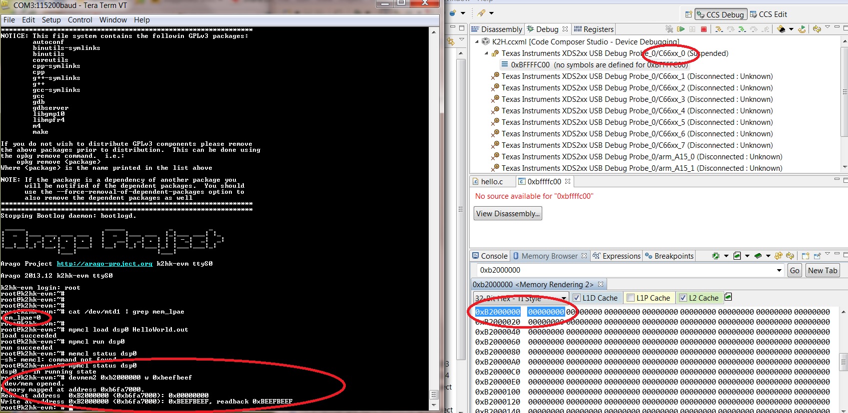
From my test it seems that DSPs are able to access DDR3A instead of DDR3B when accessing an address greater than 0x8000_0000. We are setting DDR3A_REMAP_EN=1 and I double checked it by reading the corresponding register. So, basing on my understanding of the datasheet, I should see the memory this way:

Address
ARM (DDR3A_REMAP_EN=1)
DSPs
0x00_6000_0000
DDR3B
DDR3B (alias of 0x00_8000_0000)
0x00_8000_0000
DDR3A (alias of 0x08_0000_0000)
DDR3B
0x08_0000_0000
DDR3A
DDR3A

As mentioned, when DSPs access an address in the range 0x8000_0000 - 0xffff_ffff they are able to see data written from the ARM side, which is DDR3A. For example, I write some words at 0xb200_0000 and DSP2 reads such words when accessing the same address (I am loading the DSP code by using the mpmcl command). Basing on my understanding, ARM and DSPs should work on different physical memories and they shouldn't see each others.

Is there any obvious reason that leads this behavior?

P.S. I am pretty sure that ARM is seeing the correct DDR3A memory. One thing that should confirm this is that U-boot actually puts the Linux code into the aliased memory at 0x8000_0000, Linux starts in PAE mode and it runs at physical address 0x08_0000_0000 without problems.

Thanks a lot for your support.

N.

for keystoneII TCI6638

  • Welcome to the TI E2E forum. I hope you will find many good answers here and in the TI.com documents and in the TI Wiki Pages (for processor issues). Be sure to search those for helpful information and to browse for the questions others may have asked on similar topics (e2e.ti.com). Please read all the links below my signature.

    We will get back to you on the above query shortly. Thank you for your patience.

  • Hi Raja,

    is there any update about my question?

    I spent several time by searching inside both the forum and the online documentation without luck. I am still not able to understand why our SoC is behaving this way.

    Thanks in advance for your support.

    Regards,

    N.

  • Hi, Anfz,

    The explanation of such behavior is because lpae is enabled in Linux which maps area starting at 0x8000 0000 to the first 2GB at 0x08 0000 0000, and is visible by DSP. If lpae is disabled through uboot env variable mem_lpae=0, value written by ARM at 0xc200 0000 will not be visible by DSP.

    Rex

  • Hi Rex,

    thanks for your response. What you say is pretty clear to me but I am still confused by the situation. I'll try to give a better picture of my tests.

    I start with mem_lpae=0 as suggested and DDR3A_REMAP_EN=1. So Linux is placed around 0x8000_0000 inside DDR3A and I can verify it via /proc/iomem

    From Linux I load some piece of code on DSP2 (I am not a DSP expert so I cannot go very deeply on what's inside such code). I load the code with the command "mpmcl load dsp2 dsp-code.out". Such piece of code reads 32bit located at address 0xb200_0000 and printout the read value via remoteproc.
    If I pause the DSP2 inside the CodeComposer, I am able to see the memory in a choerent way: at 0x8_0000_0000 I see the kernel code but at 0x8000_0000 I see random data. Basing on my understanding this is why DSPs see the DDR3B at 0x8000_0000 and the DDR3A at 0x8_0000_0000.

    At this point I write some data at 0xb200_0000 from the ARM side and 'magically' DSP2 prints out such data via remoteproc. I expected that DSP2 didn't see anything as ARM is writing on DDR3A while DSP is reading on DDR3B (according to the datasheet, same physical address refer to different banks when DDR3A_REMAP_EN=1 and the address is in the range 0x8000_0000 - 0xffff_ffff). According to my understanding, if I would like to read such data from DSP2, then I should access 0x8_b200_0000 address.

    To be honest, I expected that DSP2 didn't run at all as ARM is loading the DSP's code on DDR3A while DSPs see the other bank of memory.
    Is mpmcl doing some trick when loading DSP's code? Is my understanding of the memory map wrong?

    Thanks a lot for your support.

    BR,
    N.
  • Hi, Anfz,

    The DDR3A_REMAP_EN stays default which is 1 in my test. I had Linux kernel boot up with LPAE set to 1 on ARM, and then had CCS connected to DSP core 0. From kernel prompt, I entered "devmem2 0xc2000000 w 0xbeefbeef". On the CCS, I dumped memory address 0xc2000000 and can see 0xBEEFBEEF in Memory Browser. But if I disable LPAE, whatever written to the DDR3A area is not visible by DSP and the value always shows up as 0x00000000. I didn't run mpmcl, and will give it a try to see if it makes any difference.

    Rex

  • Hi, Anfz,

    I don't see the behavior as you described with lpae=0 even running mpmcl. mpmcl does not configure anything. Please see the screenshot of my test. I had kernel up and shows mpm_lpae=0 in the u-boot env variables (highlighted red circle).  A small dsp program was loaded and run. The DSP is in run state afterwards. Then, ARM modified the memory at 0xb2000000 (highlighted with red circle). Then DSP0 was connected through CCS and memory 0xb2000000 was dumped. It didn't show the value entered by ARM.


  • Hi Rex,

    I did a very similar test as yours, but apparently I get a different result. Inside the green box you can see part of the DSP code running on DSP2. Inside CCS, the memory view is the "CPU memory view" as in your case (I needed to refresh the memory to get the value written by ARM). In addition, as you can see inside the ARM console, when printing the DSP trace it seems that the DSP is able to read and print-out the right value written from the ARM side. 

  • Hi, Anfz,

    Did you run any gel file to configure DSP? Is the MPAX register configured? My target was launched without any gel file running. I'll discuss with one of my coworkers who is out on vacation and be back Monday to see what's his opinion and comment. I had an earlier discussion with others that mem_lpae only disable the linux kernel, but not DSP's capability to access space with 40-bit addressing if MPAX is configured. I want to verify with this coworker when he comes back.

    Rex

  • Hi Rex,

    I am not running any GEL file to configure DSPs. As far as I know, we are not using MPAX at all so it shouldn't be configured and related registers should hold the reset values. Is there any quick check I can make on MPAX register to see if some address translation is taking place?

    BR,
    N.
  • Hi, Anfz,

    Open your target.ccxml file in ccs by double-click the target. In the Advanced tab, select C66xx_0 and see if anything set for the initialization script. check the core you ran applicaiton on too. MPAX regsiters are in Registers View -> ControlRegisters ->XMC. I was also told that bootROM configures it but haven't been able to find out where it can be displayed.

    Rex


  • Hi Rex,

    I didn't check the MPAX register yet but I will do it as soon as possible.
    However I will try our test with a different (and simpler) DSP code which actually writes a counter at 0xb200_0000 and read what's written at 0xb200_0004. At first I got the same behavior as yours: ARM is not able to read the value of the counter at 0xb200_0000 and DSP0 is not able to read the value written by ARM at 0xb200_0004 with devmem2.

    However, after a deepest analysis I noticed that this behavior is due to the fact that DSP0 doesn't actually access to DDR3 but "stops" inside L1D cache. So, when accessing the memeory, DSP0 is actually accessing the cache instead of going down to the DDR3, so this is why ARM and DSP0 don't see each other. By inserting some 'cache invalidation' instruction inside the DSP code, ARM and DSP start to see each other through the 0xb200_0000 and 0xb200_0004 addresses (ARM is able to see the counter incremented by DSP0 and DSP0 reads all the values written by ARM via devmem2).
    Basing on this, I strongly believe that, in this moment, DSP0 accesses DDR3A when accessing 0xb200_000X addresses instead of accessing DDR3B. Here the DSP's code I used:

        while(1)
        {
            System_printf("Loop Core %d - %d\n",DNUM, mbCnt3);
    
            CACHE_invL1d((void *)ddrPointer, 128, CACHE_WAIT);
    
            memcpy((void*) ddrPointer, (void*) &mbCnt3, 4);
    
            CACHE_wbL1d((void *)ddrPointer, 4, CACHE_WAIT);
            CACHE_invL1d((void *)ddrPointer, 128, CACHE_WAIT);
            System_printf("Core0: COPY 0x%x, READ 0x%x\n", * (Uint32*)ddrPointer, *(((Uint32*)ddrPointer)+1) );
    
            for (mbCnt=0;mbCnt<1000000;mbCnt++)
            {
                for (mbCnt2=0;mbCnt2<500;mbCnt2++);
            }
            mbCnt3++;
    
            if (0xFFFFFFFF == mbCnt3)
            {
                 mbCnt3 = 1;
            }
    
        }

  • Hi Rex,

    It seems that I figured out the root cause of the 'problem'. Actually XMC/MSMC registers configure the mapping DDR3B->DDR3A when they go out of the reset state. Therefore the DSP cores will see the DDR3A bank when addressing [0x8000_0000, 0xffff_ffff] until such registers are set up properly.

    Anyway, now I am facing another issue. Basing on the fact that ARM runs on DDR3A and DSPs on DDR3B, is it possible to load the DSP's code on DDR3B via mpmcl?

    Currently I have a DSP code that has some sections in L2SRAM, some sections in MSMCSRAM and some section in DDR3. I'd like that ARM would load the DDR3 section into DDR3B instead of DDR3A as DPSs will work on that memory bank.

    I tried different configuration inside the mpm_config.json file but it seems that mpmcl loads the DDR3 section of DSP's code on DDR3A overlapping the Linux's code (causing a kernel crash) instead of loading them on DDR3B.

    I am suspecting that what I am trying to do is not possible at all with mpmcl.

    BR,

    N.

  • Hi, Anfz,

    Glad that you resolve the addressing issue. ARM can load the DSP code to the area of 0x6000 0000 - 0x7FFF FFFF which is DDR3B for both ARM and DSP. As described in data sheet, "This region is aliased of 00 0800 0000 to 00 9FFF FFFF (the first 512MB of DDR3B)."

    Rex

  • Hi Rex,

    thanks again for your help.

    I am aware of the "shared memory view" located at 0x6000_0000 - 0x7FFF_FFFF and I am able to use it without problems. The fact is that we have a lot of code running on DSP (i.e., a lot of sections to be loaded on DDR3B) and, by using that address space, I can load only 512 MiB of code on DDR3B memory bank. The other 1,5GiB of DDR3B will be unused as we can't load any sections in there from ARM side (via mpmcl).

    So, it seems that we don't have any chance to load any code on DDR3B at address higher than 512MiB via mpmcl and we have to continue to use the DDR3A memory for DSPs code.

    BR,

    N.

  • Hi, Anfz,

    If that is the case, I am afraid that DDR3A is the solution.

    Rex