


Hi e2e team,
We are working on custom board based on 66AK2E05 processor , with following hardware modifications/differences from 66AK2E05 EVM reference board.
1. Security accelerator enabled processor with 66AK2E05XABD4 manufacture part number.
2. Our Custom board has 2GB DDR3 (part num: MT41J256M16HA-125:E) on board, Sinlge RANK, 1600 Speed Grade, 64 bit bus width (16bit x 4 Device). Where as EVM has 4GB DDR3 SO-DIMM (part num: MT18KSF51272HZ-1G6)
Currently in board bring up phase and now facing issue in accessing the DDR3 memory locations using CCS Memory browser option, after loading GEL file.
Attached is the GEL file which located in the below patch, after installing CCS6 (ccs_setup_6.1.1.00022):
"ccsv6\ccs_base\emulation\boards\evmk2e\gel\evmk2e.gel"
Followed the below steps to Load the GEL file into our custom board
1. Opened the CCS and connected to the below Target configurations
"Texas Instruments XDS2xx USB Onboard Debug Probe -> 66AK2E05"
and launched the configurations
2. Loaded the ättached GEL file to the core " Texas Instruments XDS2xx USB Onboard Debug Probe_0/C66x_0"
3. Right clicked on the "Texas Instruments XDS2xx USB Onboard Debug Probe_0/C66x_0" and selected "Connect Target" option.
4. Then GEL file was loaded successfully without any error, attached[gel_load_log.txt] is the console message of GEL file loading
		C66xx_0: GEL Output:
		Connecting Target...
		C66xx_0: GEL Output: TCI6636K2E GEL file Ver is 1.1
		C66xx_0: GEL Output: Detected PLL bypass enabled: SECCTL[BYPASS] = 0x00800000
		C66xx_0: GEL Output: (2a) MAINPLLCTL1 = 0x00000040
		C66xx_0: GEL Output: (2b) PLLCTL = 0x00000048
		C66xx_0: GEL Output: (2c) PLLCTL = 0x00000048
		C66xx_0: GEL Output: (2d) Delay...
		C66xx_0: GEL Output: (2e) SECCTL = 0x00810000
		C66xx_0: GEL Output: (2f) PLLCTL = 0x0000004A
		C66xx_0: GEL Output: (2g) Delay...
		C66xx_0: GEL Output: (2h) PLLCTL = 0x00000048
		C66xx_0: GEL Output: (4)PLLM[PLLM] = 0x00000013
		C66xx_0: GEL Output: MAINPLLCTL0 = 0x05000000
		C66xx_0: GEL Output: (5) MAINPLLCTL0 = 0x09000000
		C66xx_0: GEL Output: (5) MAINPLLCTL1 = 0x00000040
		C66xx_0: GEL Output: (6) MAINPLLCTL0 = 0x09000000
		C66xx_0: GEL Output: (7) SECCTL = 0x00890000
		C66xx_0: GEL Output: (8a) Delay...
		C66xx_0: GEL Output: PLL1_DIV3 = 0x00008002
		C66xx_0: GEL Output: PLL1_DIV4 = 0x00008004
		C66xx_0: GEL Output: PLL1_DIV7 = 0x00000000
		C66xx_0: GEL Output: (8d/e) Delay...
		C66xx_0: GEL Output: (10) Delay...
		C66xx_0: GEL Output: (12) Delay...
		C66xx_0: GEL Output: (13) SECCTL = 0x00090000
		C66xx_0: GEL Output: (Delay...
		C66xx_0: GEL Output: (Delay...
		C66xx_0: GEL Output: (14) PLLCTL = 0x00000041
		C66xx_0: GEL Output: PLL has been configured (CLKIN * PLLM / PLLD / PLLOD = PLLOUT):
		C66xx_0: GEL Output: PLL has been configured (100.0 MHz * 20 / 1 / 2 = 1000.0 MHz)
		C66xx_0: GEL Output: Power on all PSC modules and DSP domains...
		C66xx_0: GEL Output: Power on all PSC modules and DSP domains... Done.
		C66xx_0: GEL Output: WARNING: SYSCLK is the input to the PA PLL.
		C66xx_0: GEL Output: Completed PA PLL Setup
		C66xx_0: GEL Output: PAPLLCTL0 - before: 0x0x098804C0	 after: 0x0x090804C0
		C66xx_0: GEL Output: PAPLLCTL1 - before: 0x0x00000040	 after: 0x0x00002040
		C66xx_0: GEL Output: DDR begin
		C66xx_0: GEL Output: XMC setup complete.
		C66xx_0: GEL Output: DDR3 PLL (PLL2) Setup ...
		C66xx_0: GEL Output: DDR3 PLL Setup complete, DDR3A clock now running at 800 MHz.
		C66xx_0: GEL Output: DDR3A initialization complete
		C66xx_0: GEL Output: DDR done
In the gel_load_log.txt file , PLL clock initialization, PSC modules and DSP domains power Enable, DDR3 initialization has been done in the GEL file.
Please let us know if there is any specific initialization is required other than this.
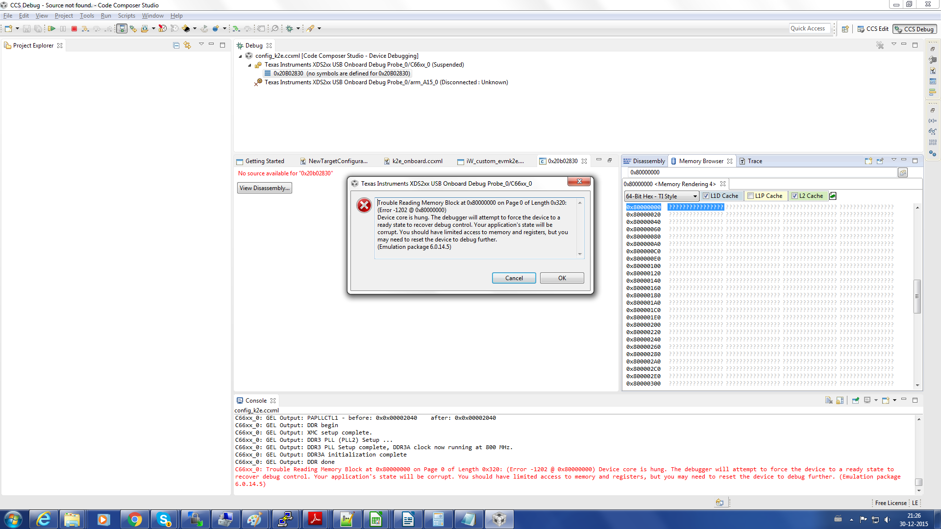
5. After GEL file is loaded, to verify whether RAM is initialised properly, opened "View->Memory Browser" and try to view the contents of DDR3 Start Address "0x80000000"
Encountered the following error: "Trouble Reading Memory Block at 0x80000000 on Page 0 of Length 0x320:(Error -1202 @ 0x80000000)" and device got hung. we are facing the same issue while accessing some of the other register
ex: 0x21010200.
This beheviours is not observed with the 66AK2E05EVM with the same GEL file [evmk2e.gel].
Please find the attached ddr3_8000000_readerror.png error for your reference.
Got stuck with this and could nott able to figure out what is the cause of this memory read failure.
Is the error, because of the GEL file which we are using ? what possibly cause of this issue ? also let us know is there any other GEL file for 66AK2E05.
Verified Proper power up sequence of the processor, by checking the RESETSTAT and SYSCLK output from the device.
Provided dip switch for selecting the BOOT modes. Please let us know the exact configuration that has to be provided through dip switch while using in the CCS debugger mode. Can u please provide the Boot configuration
pin values which is being used in 66AK2E05 EVM (Since boot pin configuration will be provided through BMC in EVM).
Thanks & Regards,
Sarjoon.


