This thread has been locked.

If you have a related question, please click the "Ask a related question" button in the top right corner. The newly created question will be automatically linked to this question.

[OMAPL138] DDR Physical layout

Other Parts Discussed in Thread: OMAP-L138

DDR routing question

My question has to do with determining the 'Target' length of my routes for the net class that is referred to in Table 6-35 on page 123 of OMAP-L138 Low-Power Applications Processor (SPRS586A–JUNE 2009–REVISED AUGUST 2009). I need to know how to correctly interpret item 4 for 'CACLM' which refers to the 'longest Manhattan distance of the CK and ADDR_CTRL net classes'.

On my board the longest route in this net class is less than the 'longest Manhattan distance of the CK and ADDR_CTRL net class' (which would be measured between the pair of pins farthest from each other in this 'net class' that run between the 2 devices).

Can this shorter length be used or do I need to add extra length to this route (and all the others) to match the actual Manhattan distance I measured from pin to pin?

I would prefer to not add extra length as the routing is already congested. Thanks for any assistance.

TI_OMAP-L138_pg123.pdf
  • It is ok to be shorter than the CACLM, so you dont need to add extra lengths to all the traces. This was mainly for when 2 DDR devices are used to make sure the balanced T structure is kept. For a single memory, you should route as short as possible while maintaining skew matching.

    Jeff

  • I think I understand this, but I just want to be sure.

    Even if I only have a single DDR2 memory chip, I need to match all signals within the same group within 100 mils.  That means that if one of my address lines is 310 mils, the longest address line (or any line in the ADDR_CTRL group) can be is 410 mils. 

    I have traces that will route in the 300s, but some will take 600 mils. I'm just going to a single IC right next to the DSP.  So I'm going to end up with major serpentine traces.  Some traces may need almost to double in length.  Is this right?

    Thanks,

    CJ

  • Yes that is correct. Even for single chips, the skew matching requirements must be followed.

    Jeff

  • Thank you for your rapid reply.

    Have you seen a board with short traces twice as long as they need to be?  I want to make sure I'm not doing something foolish. 

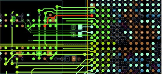
    Look how nice that red trace looks.  I'm going to have to double its length at least.

    Also, are there any guidelines about how tight the switchbacks can be?  That is most likely up to the engineer.  It means I have to worry about inductive coupling reducing the amt of delay and capacitive coupling fouling up the eye diagram.

  • While I agree that the highlighted trace is ascetically pleasing that is not what matters most here.  Folded back serpentine routes are par for the course for DDR routing.  DDR uses a source synchronous bus thus what really controls input setup and hold is the skew between the clock at the information being sent.  The only way to equalize the length of traces in a bus is to extend them all out the the longest one of the net class and clock.

    The way to optimize the route is to ensure the longest route of the address/control bus is a short as possible.  This will minimize the added length needed to length match the bus.  One advantage you have with the tight placement shown above is you can likely get away with minimum spacing for almost all of it.  You are allowed to route the nets at minimum spacing for up to 500 mils of routed length.  This is intended for BGA escapes and routing congestion.  This applies to the serpintined traces as well.

    With respect to the length added traces, I would maintain a 4w spacing in between the cycles to minimize self cross talk.  If the entire length of the net is near 500 mils, you will likely be able to route the whole thing at minimums, including the serpentine cycles.   You do not need to worry about inductive or capacitive coupling provided you are following the layout spec.

    Also, do not attempt to length match the entire bus.  You only need to length match CK to ADDR/CTRL, DQS0 to byte 0, and DQS1 to byte 1.  Do not match across the clock domains.


    -Mike

  • Thank you for helping me with this and for giving more help on the phone.


    What do you think if one of my reference planes is 1.8V?  Is that as good as ground, provided I have good decoupling spread around the area?

  • The reference planes for this design must be ground planes as per the spec.  You can use a ground sub-plane under the DDR routing region.  Just make sure there are no cuts in it.  At the edges of the sub-plane, ensure no adjacent layer traces cross the boundary.

    -Mike

  • Michael Shust said:

    The reference planes for this design must be ground planes as per the spec.  You can use a ground sub-plane under the DDR routing region.  Just make sure there are no cuts in it.  At the edges of the sub-plane, ensure no adjacent layer traces cross the boundary.

    I certainly never would cross a cut with a high-speed signal.  My question is whether it's okay for the plane or sub-plane to be 1.8V instead of ground.  My idea is that 1.8V is as good a ground from an AC point-of-view as long as I have good highs-speed decoupling throughout the area. 

    Do you have reports that a well-decoupled power plane does not perform as well as a ground plane for DDR?