This thread has been locked.

If you have a related question, please click the "Ask a related question" button in the top right corner. The newly created question will be automatically linked to this question.

problem when writing data on emifa 8 bit from C6748 on OMAP L138 LCDK board

Other Parts Discussed in Thread: OMAPL138, OMAP-L138

Hi there,

Did anyone have this problem writing data on 8 bit  EMIFA bus from C6748 ( on OMAPL138 LCDK board)?

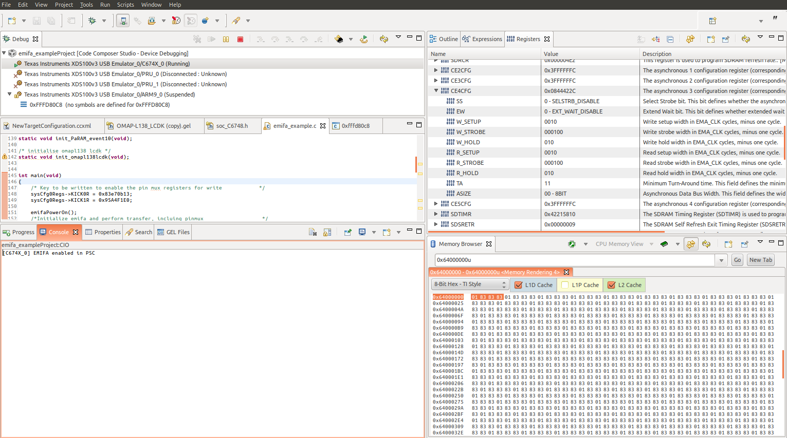
My emifa bus is using CS4. Basically, when writing data from 0x01 to 0xff in normal mode , I don't see correct data on my  oscilloscope. see picture below.  My aim is to connect my LCDK to a FPAG.

As I see, EMA_CS4 pin, OEn pin and WE pin work correctly. I also checked EMA_A/ BA1 / BA0  bus by swapping data pin and they appearred to work correctlyas well.

I cannot find any problems in configuration of EMIFA CS4 in 8 Bit. Can anyone help me here? 

  • Hi,

    We will work on this and will update you shortly.

    Thanks & regards,
    Sivaraj K
  • Hi Sivaraj Kuppuraj, many thanks in advance. As this becomes a blocking issue for us, it is really appreciated if you can help us soon. We are reading EMIFA interface which will be connected to an 8 bit ADC output and 8 bit DAC input. Once EMIFA works correctly on OMAPL138, we will connect OMAPL138 to our 8 bit ADC/DAC device.

    Cheers,
    Louie
  • Yi Lu,

    We do not have such issue with the EMIFA interface. I suspect on the EMIFA configurations, could you please share the software that you are using for this test.

    Are you seeing the correct data written on the CS4 memory space ?

    Regards,
    Senthil
  • Dear Senthil,

    Thanks for your quick reply. Sure, I copy and post the code I used for this test. Please help check my configuration. (As I am new to C6748, I could not find any problem here). 

    Below is how I write test values on emifa bus

    Uint8 cnt = 0x00;

    volatile Uint8 * cs4_ptr = ( volatile Uint8 *)(0x64000000u); //(CSL_EMIFA_CS4_ADDR);

    while (cnt < 0xff ){ cs4_ptr[cnt] =cnt; cnt++; }

    Below is my configuration

    enum bus_width {
    bit8,
    bit16,
    bit32
    };
    enum bus_width emifa_bus;
    emifa_bus = bit8;
    //emifa_bus = bit16;

    if (emifa_bus == bit8) {
    /* configure the pinmux for the EMIFA */
    //////////////////////////////
    // 8 bits
    /////////////////////////////////
    /*
    * EMIFA to 8 bit fpga interface
    *
    * DSP FPGA
    *
    * EMA_CLK ---> EMA_CLK
    * EMA_D[7:0] <--> DQ[7:0]
    * EMA_A[x:0] ---> A[x+2:2]
    * EMA_BA[1:0] ---> A[1:0]
    * EMA_OE --->
    * EMA_WE_DQM --->
    * EMA_WE --->
    * EMA_CS[4] --->
    */

    // PINMUX5 --- config EMA_BA[1:0]
    sysCfg0Regs->PINMUX5 = (( CSL_SYSCFG_PINMUX5_PINMUX5_31_28_EMA_BA0 << CSL_SYSCFG_PINMUX5_PINMUX5_31_28_SHIFT) |
    ( CSL_SYSCFG_PINMUX5_PINMUX5_27_24_EMA_BA1 << CSL_SYSCFG_PINMUX5_PINMUX5_27_24_SHIFT));

    // PINMUX6 --- config EMA_CS[0]/WAIT[1]/WE_DQM[1:0]/CLK
    // gpio2_0
    //tmp = (sysCfg0Regs->PINMUX6 & 0xF0FFFFF0) | 0x01000001;
    sysCfg0Regs->PINMUX6 = tmp;
    sysCfg0Regs->PINMUX6 = (
    (CSL_SYSCFG_PINMUX6_PINMUX6_27_24_EMA_WAIT1 << CSL_SYSCFG_PINMUX6_PINMUX6_27_24_SHIFT) |
    (CSL_SYSCFG_PINMUX6_PINMUX6_23_20_NEMA_WE_DQM1 << CSL_SYSCFG_PINMUX6_PINMUX6_23_20_SHIFT) |
    (CSL_SYSCFG_PINMUX6_PINMUX6_19_16_NEMA_WE_DQM0 << CSL_SYSCFG_PINMUX6_PINMUX6_19_16_SHIFT) |
    (CSL_SYSCFG_PINMUX6_PINMUX6_3_0_EMA_CLK << CSL_SYSCFG_PINMUX6_PINMUX6_3_0_SHIFT));


    // PINMUX7 --- config EMA_WAIT[0]/A_RW/OE/WE/CS[5]/CS[4]/CS[3]/CS[2]
    // tmp = (sysCfg0Regs->PINMUX7 & 0x0000FFF0) | 0x11110001;
    // sysCfg0Regs->PINMUX7 = tmp;
    sysCfg0Regs->PINMUX7 = (
    (CSL_SYSCFG_PINMUX7_PINMUX7_23_20_NEMA_OE << CSL_SYSCFG_PINMUX7_PINMUX7_23_20_SHIFT) |
    (CSL_SYSCFG_PINMUX7_PINMUX7_19_16_NEMA_WE << CSL_SYSCFG_PINMUX7_PINMUX7_19_16_SHIFT) |
    (CSL_SYSCFG_PINMUX7_PINMUX7_11_8_NEMA_CS4 << CSL_SYSCFG_PINMUX7_PINMUX7_11_8_SHIFT));


    // PINMUX8 --- config GPIO3_0/1/2/3/4/5/6/7 <--- EMA_D[15:8]
    sysCfg0Regs->PINMUX8 = 0x88888888;
    // tmp = (sysCfg0Regs->PINMUX8 & 0x00000000) | 0x11111111;
    // sysCfg0Regs->PINMUX8 = tmp;


    // PINMUX9 --- config EMA_D[0]/D[1]/D[2]/D[3]/D[4]/D[5]/D[6]/D[7]
    tmp = (sysCfg0Regs->PINMUX9 & 0x00000000) | 0x11111111;
    sysCfg0Regs->PINMUX9 = tmp;
    //sysCfg0Regs->PINMUX9 = 0x11111111;

    // PINMUX10 --- config
    sysCfg0Regs->PINMUX10 = 0x22222222;
    // tmp = (sysCfg0Regs->PINMUX10 & 0xFFFFFFFF) | 0x00000000;
    // sysCfg0Regs->PINMUX10 = tmp;

    // PINMUX11 --- config GP5_8/9/10/11/12/13/14/15
    //sysCfg0Regs->PINMUX11 = 0x88888888;
    tmp = (sysCfg0Regs->PINMUX11 & 0x000000FF) | 0x88888800;
    sysCfg0Regs->PINMUX11 = tmp;

    // PINMUX12 --- config EMA_A[0]/A[1]/A[2]/A[3]/A[4]/A[5]/A[6]/A[7]
    // sysCfg0Regs->PINMUX12 = 0x11111111;
    tmp = (sysCfg0Regs->PINMUX12 & 0x00000000) | 0x11111100;
    sysCfg0Regs->PINMUX12 = tmp;

    Uint32 val_revid = emifaRegs->REVID;
    emifaRegs->CE4CFG =
    (CSL_EMIFA_CE4CFG_SS_SELSTRB_DISABLE << CSL_EMIFA_CE4CFG_SS_SHIFT)
    | (CSL_EMIFA_CE4CFG_EW_EXT_WAIT_DISABLE << CSL_EMIFA_CE4CFG_EW_SHIFT)
    | (CYCLE2 << CSL_EMIFA_CE4CFG_W_SETUP_SHIFT)
    | (CYCLE2+1 << CSL_EMIFA_CE4CFG_W_STROBE_SHIFT)
    | (CYCLE2 << CSL_EMIFA_CE4CFG_W_HOLD_SHIFT)
    | (CYCLE2 << CSL_EMIFA_CE4CFG_R_SETUP_SHIFT)
    | (CYCLE2+1 << CSL_EMIFA_CE4CFG_R_STROBE_SHIFT)
    | (CYCLE2 << CSL_EMIFA_CE4CFG_R_HOLD_SHIFT)
    | (CYCLE2 << CSL_EMIFA_CE4CFG_TA_SHIFT)
    | (CSL_EMIFA_CE4CFG_ASIZE_8BIT << CSL_EMIFA_CE4CFG_ASIZE_SHIFT);

    }

    Many thanks,

    Louie

  • Louie,

    We will review your code and get back.

    Regards,
    Senthil
  • Many thanks Senthil,
    Louie
  • Hi Senthil,

    I am just wondering if there are any registers in pscCfg which are related to pinmux for EMIFA. I pasted emifa power on function below and could you please also check if there is problem there.  

    static void emifaPowerOn(void)
    {
    volatile Uint32 pscTimeoutCount = 1024u;
    Uint32 temp = 0;

    /*
    * need to power on emifa module in the psc
    */
    psc0Regs->MDCTL[CSL_PSC_EMIFA] = ((psc0Regs->MDCTL[CSL_PSC_EMIFA]&0xFFFFFFE0)| CSL_PSC_MDSTAT_STATE_ENABLE);

    /*
    * kick start the enable command
    */
    temp = psc0Regs->PTCMD;
    temp = ((temp & CSL_PSC_PTCMD_GO0_MASK)| (CSL_PSC_PTCMD_GO0_SET << CSL_PSC_PTCMD_GO0_SHIFT));

    psc0Regs->PTCMD |= temp;

    while (((psc0Regs->PTSTAT & (CSL_PSC_PTSTAT_GOSTAT0_IN_TRANSITION))!= 0)
    && (pscTimeoutCount>0))
    {
    pscTimeoutCount--;
    }

    /*
    * check if PSC state transition timed out
    */
    if (0 == pscTimeoutCount)
    {
    printf("EMIFA PSC transition to ON state timed out \n");
    } else {
    printf("EMIFA enabled in PSC\n");
    }
    }

    Cheers,

    Louie

  • Dear Louie,
    I would like to suggest you to use the following NAND examples from starterware and flash tools package as already it has PINMUX and configurations.
    C:\ti\OMAPL138_StarterWare_1_10_04_01\examples\lcdkOMAPL138\nand
    C:\ti\OMAP-L138_FlashAndBootUtils_2.40\OMAP-L138\CCS\NANDWriter

    You can also cross verify the PINMUZ registers and EMIFA timing registers through "CCS register" window.

    Ex:

    #define EMIF_CS4 *(unsigned int *) 0x64000000

    int main(void)
    {
    int blkNum;
    int pageNum;
    int numOfPages;
    unsigned int retVal;
    unsigned int eraseBlkFlg;

    /* NAND structure allocations for this application */
    NandInfo_t nandInfo;
    NandCtrlInfo_t nandCtrlInfo;
    NandEccInfo_t nandEccInfo;
    NandDmaInfo_t nandDmaInfo;
    EMIFANANDTimingInfo_t nandTimingInfo;

    /* Initializing the UART instance for serial communication. */
    UARTStdioInit();

    UARTPuts("\r\n ************* StarterWare NAND Application ************"
    "\r\n\r\n", -1);

    /* Pin mux and clock setting */
    EMIFAClkConfig();
    NANDPinMuxSetup();

    /* Initialize the nandInfo struct */
    nandCtrlInfo.hNandTimingInfo = (void *) &nandTimingInfo;
    nandInfo.hNandCtrlInfo = &nandCtrlInfo;
    nandInfo.hNandEccInfo = &nandEccInfo;
    nandInfo.hNandDmaInfo = &nandDmaInfo;
    NANDInfoInit(&nandInfo, NAND_CHIP_SELECT);

    /* Open the NAND device */
    retVal = NANDOpen(&nandInfo);
    if (retVal & NAND_STATUS_FAILED)
    {
    UARTPuts("\r\n*** ERROR : NAND Open Failed... ",-1);
    while(1);
    }
    else if (retVal & NAND_STATUS_WAITTIMEOUT)
    {
    UARTPuts("\r\n*** ERROR : Device Is Not Ready...!!!\r\n", -1);
    while(1);
    }
    else if (retVal & NAND_STATUS_NOT_FOUND)
    {
    UARTPuts("\r\n*** ERROR : DEVICE MAY NOT BE ACCESSABLE OR NOT PRESENT."
    "\r\n", -1);
    while(1);
    }
    else if(nandInfo.devId != NAND_DEVICE_ID)
    {
    /* Check if detected ID matches supplied ID */
    UARTPuts("\r\n*** ERROR : INVALID DEVICE ID.", -1);
    while(1);
    }
    else
    {
    /* Print The Device ID info */
    NANDDeviceIdInfoPrint(&nandInfo);
    }

    #ifdef NAND_DATAINTEGRITY_TEST_WITH_FIXED_ADDR
    /* Do read/write for predefined address */
    pageNum = NAND_DEFAULT_START_PAGE;
    blkNum = NAND_DEFAULT_BLK;
    numOfPages = NAND_DEFAULT_NMBR_OF_PAGES;
    #else

    //Titus
    while(1)

    {

    // *(unsigned int *EMIF_CS4) = 0xFF;

    EMIF_CS4 = 0xFF;

    EMIF_CS4 = 0x00;

    // *(unsigned int *EMIF_CS4) =0x00;

    // *(unsigned short *)0x64000000 = 0xFF;
    // *(unsigned short *)0x64000000 = 0x00;

    }


    I am just wondering if there are any registers in pscCfg which are related to pinmux for EMIFA. I pasted emifa power on function below and could you please also check if there is problem there.

    I don't see any issues here, pscCfg register is used to power up the EMIFA peripheral (enable the EMIFA module clock)
  • Hi Titusrathinaraj,

    Thanks for your reply and I will try what you suggested and then let you know.

    On the other hand, I saw something strange about voltage of these EMIFA PINs when I was running test using different configuration or data being written in CS4 memory. 

    1/ Just to check if there is any register which controls voltage of these PINs?

    2/ by default, are these PINs LVCMOS33? if not, could you please let me know what they are then? (as I cannot find any document which describe them.)

    Cheers,

    Louie

  • Louie,

    1. There is no register to control the voltage of the EMIF pins.

    2. Yes, these pins are LVCMOS33 logic levels.

    Regards,
    Senthil
  • Hi Senthil,

    OK it could be some unknown problems in my configuraiton. But, as you have seen my code above, no problems are seen. So, I am still feeling a bit strange about my problem. Just to check if nand configuration could cause my problem here? as nand is also using EMIFA interface. Looking at boot up prints when switching on OMAPL138 LCDK, there are nand related prints. In uboot, it seems that these EMIFA pins are configured for nand by default so that they cannot be reprogrammed in order to achieve what I am trying to do here.

    Also, looking at my gel file, PINMUX7/9... are configured for nand.

    Do you think if I need to disable pinmux for nand in uboot or gel file or other related places?

    Cheers,
    Louie
  • Hi Senthil,

    Thanks for your answer earlier on. Just to check if my problem could be caused by nand?

    I am seeing it is trying to detect nand when switching my omapl138 lcdk on. As emifa is also used by nand, do I need to disable nand in uboot or kernel etc?. I also see emifa pinmux is configured for nand in my gel file.

  • How you are testing the code ?
    After booting Linux or debugging the code via CCS ?

    What boot mode are you using while testing/running the code ?

    Please set boot mode to UART to made sure that EMIF pins were untouched.

    Yes, its better to remove the EMIF initialization part in u-boot and kernel if you have your own EMIFA code.
  • Hi Titus S,

    I will run my EMIFA code in uart mode and then update you.

    Cheers,
    Louie
  • Dear Louie,
    If you run your EMIFA code with UART mode then RBL won't touch EMIFA part.
    Please update to us if you got something.
  • Dear Titus S,

    I ran my EMIFA test code in uart mode and started seeing emifa pins behave strangely. Without read/write to CS4 memory, it was seen that signals on WEn and OEn and CS4 were on and off continuously. please see attached screen shot below.

    Then checking CS4 memory in memory browser, it appeared that there were data there, which is a bit odd. I am just wondering if you have seen things like this before? BTW, I have attached my gel file when loading arm core.OMAP-L138_LCDK (copy).gel

  • Dear Titus S,

    Hope you had a good weekend.

    I am just wondering if you had a chance to have a look at our issue. I had another look at it over weekend. Unfortunately, I could not find why cs4 memory had data before writing anything into it.

    Cheers,

    Louie

  • Dear Louie,
    Which boot mode have you set while running the EMIFA code ?
    Please use UART boot mode for debugging code on CCS.
  • Dear Titus S,

    I was running in uart mode.

    Louie
  • Dear Titus S,

    It is very strange problem here. I enabled memory analysis. please see a screenshot below. 

    I am new to CCS. Does it mean that L2/L1 cache have these strange value? where are these values from?

    (i am running it in uart mode)

    Cheers, Louie

  • Dear Louie,
    Don't put tick the L1/L2 cache option in CCS unless you enable and use the cache in code.
    What value you are getting when you haven't enable the cache in CCS ?

    If you want to test the EMIFA, then we have connected NAND flash on OMAPL138/C6748 LCDK boards which has 16bit NAND.

    You can run the examples.
    C:\ti\OMAPL138_StarterWare_1_10_04_01\examples\lcdkOMAPL138\nand
    C:\ti\OMAP-L138_FlashAndBootUtils_2.40\OMAP-L138\CCS\NANDWriter