This thread has been locked.

If you have a related question, please click the "Ask a related question" button in the top right corner. The newly created question will be automatically linked to this question.

AM437x USB HUB Design

My cusotomer is designing AM437x USB Host + USB Hub system from following informations.
- Wiki
processors.wiki.ti.com/.../AM437x_Schematic_Checklist
- e2e USB interface
e2e.ti.com/.../804511
- e2e USB host without VBUS and DRVVBUS
e2e.ti.com/.../239776
- e2e USB Host with USBHUB operation
e2e.ti.com/.../1281293

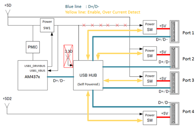
The block block diagram is like follows.

AM437x.USB1 is USB Host and AM437x.USB0 is used for USB Device although USB0 is not on block diagram.
+5D is source power for VBUS of Port1,2,3.
+5D2 is source power for VBUS of Port4
+5D and +5D2 have no relation each other.
AM437x.USB1.DRVVBUS and AM437x.USB1.VBUS can manage +5D but can not manage +5D2.

Is this design OK ? or what should be applied for good design ?

Regards,
Takeshi Matsuzaki

  • Hi,

    This should work. If your customer requires a schematic review, you can request it through local TI FAE.
  • Please ensure that the 5D2 rail is active/stable prior to assertion of DRVVBUS.

    Most (all?) hubs have a VBUS_DETECT pin. This should be connected to the output of the power switch controlled by DRVVBUS. Please note that in some cases this is a 3.3V input to the hub so a voltage translator or R-divider from 5V may be needed here.

  • Hi DK,
    Thanks for good suggestion.

    > Please ensure that the 5D2 rail is active/stable prior to assertion of DRVVBUS.

    OK, My customer ensures +5D2 is active/stable prior to assertion of DRVVBUS.

    By the way, he noticed that the Power SW driven by AM437x.USB_DRVVBUS1 should be big one(500mA+500mA+500mA..).
    So he add some changes to the circuit like follows.

    +5D goes to the Power SW of Port1,2,3 straight.
    Power SW1 drives USB1_VBUS and power source of USB_HUB, so Power SW1 could be small.
    The Power SW of Port1,2,3 is enabled by USB HUB and USB HUB start to work after USB_DRVVBUS1enables the Power SW1.
    Of course +5D2 comes befor +5D.

    Is this OK??

    Regards,
    Takeshi Matsuzaki.

  • I agree, this is a better circuit topology. They may be able to use a simple two FET discrete circuit for SW1 since there is no requirement to limit current for this on-board USB port.

    Please refer to the following E2E post for an example of this circuit.
    e2e.ti.com/.../1281293

    Regards,
    Paul
  • Paul, DK,
    Thanks a lot. My customer satisfied with your help.

    Regards,
    Takeshi Matsuzaki