This thread has been locked.

If you have a related question, please click the "Ask a related question" button in the top right corner. The newly created question will be automatically linked to this question.

[C5535] Usage of SAR ADC

Guru 24520 points

Hi TI Experts,

Please let me confirm the usage of SAR ADC on C5535.

Would you please teach me the registers to use the GPAIN0 pin?

My customer would like to use the following path. So they would like to know the register settings to use this path.
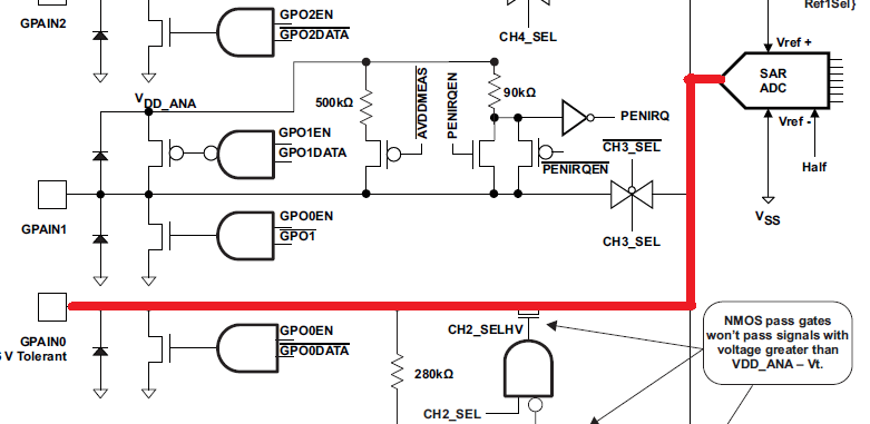
---------Edit --------

I confirmed the customer's settings for SAR resisters.

  SARCTRL: 0xA000

 SARCLKCTRL:0x0031

   SYSCLK: 98MHz

 SARPINCTRL:0x3102

 SARGPOCTRL:0x0000

If you find any problem for this values, please let me know.

If you have any questions, please let me know.

Best regards.

Kaka

  • Hi Kaka-san,

    What would be the input voltage at GPAIN0 ?  could you please let us know.

    Regards
    Vasanth

  • Hi Vasanth,

    The assumed maximum input voltage for GPAIN0 is 1.43V.
    Customer adjust the this input voltage by adding the voltage dividing resisters.

    Best regards.
    Kaka
  • Hi Vasanth,

    Please let me confirm the following question in addition to my above request.
    We can use the CH2 by set the bit2 on SARPINCTRL. According to the other E2E thread, this bit uses for the controlling the NoHV.
    Now we showed the registers as below to my customer in order to use the CH2
    *************************
     SARCTRL: 0xA000
     SARCLKCTRL:0x0031
     SARPINCTRL:0x3106
     SARGPOCTRL:0x0000
    **************************
    We have some questions for this settings.
    [Question.1]
    To read the CH2, we can read the CH2 even though the bit of GNDON on SARPINCTRL is cleared.
    Is my understanding correct?

    [Question.2]
    If we set the bit 2 on SARPINCRT, is there any problem to read the value of CH3?
    Customer would like to use the same register value of SARPINCTRL when read the CH3.

    [Question.3]

     Would you please teach the means of "Vt" at the formula of "VDD_ANA-Vt" on Figure 11-1. SAR Converter?


    If you have any questions, please let me know.
    Best regards.
    Kaka

  • Hi Kaka-san,

    If the input voltage is bigger than VDDA_ANA, then channel 2 will be disabled and channel 1 has to be used. The gate of those NMOS transistor is driven by VDD_ANA and NMOS pass gates  won’t pass signals with voltage greater than VDD_ANA – Vt.

    To illustrate this further, say in channel 2 case,  if GPAIN0 input is 3.6V (for example) then the source is 3.6V & the gate is at 1.3V.  So Vgs = 1.3 – 3.6V = -2.3. So with this voltage channel2 transistor will be off.

    Below are my response for your other questions:

    Q1: To read the CH2, we can read the CH2 even though the bit of GNDON on SARPINCTRL is cleared. Is my understanding correct?

    Vasanth: The Channel 2 criteria is explained above.


    Q2: If we set the bit 2 on SARPINCRT, is there any problem to read the value of CH3? Customer would like to use the same register value of SARPINCTRL when read the CH3.


    Vasanth: You mean GNDON bit ?  If so, then as mentioned in the datasheet – “GNDON - Ground SAR Analog Channel 0 and introduce a voltage resistor divider network in SAR Channel 1 “. As per my knowledge, this shouldn’t have effect on Channel3, as GNDSW is to introduce resistor divider for channel 1 as shown in Figure 11-1. SAR Converter .

    Hope this clarifies.


    Regards

    Vasanth

  • Hi VAsanth,

    Thank you for your kindly response. But I could not clear my concerns.
    Would you please confirm the following question.

    Q1. According to the TRM, the NoVH must be "1" to measure ch2.
    So, if we would like to use the CH2, we need to disable the NoVH.
    And according to the following E2E thread, the NoVH control bit is bit 2(Reversed bit) on SARPINCTRL.
    e2e.ti.com/.../326102
    >[Q]
    >I have confirmed that the conversion fails if bit 2 is not set despite the fact that bit 2 is "reserved" according to table 11-6 in the technical >reference manual. Is this behavior documented somewhere?
    >[ANS]
    >This is to disable the high voltage protection circuits which prevent conversion when the analog voltage (AVdd) is lower than the voltage at >the GPAIN0 pin; and the maximum allowed voltage at the GPAIN0 pin is 3.6V. Can you check the voltages you have?

    Is my understanding correct?

    Q2. If disabled the NoVH feature, will be the channel 2 disabled if the input voltage is bigger than VDDA_ANA?

    Q3. If we set the bit 2(Control NoVH Enable/Disable) on SARPINCRT, is there any problem to read the value of CH3?
    Customer would like to use the same register value of SARPINCTRL when read the CH3.

    Q4. Would you please teach the means of "Vt" at the formula of "VDD_ANA-Vt" on Figure 11-1. SAR Converter?

    Q5. How much is the maximum "VDD_ANA - Vt" voltage in consideration of the variation when the NoVH is disabled?

    Q6.According to the datasheet of C5535 on page 35, the GPAIN0 pin is unable to accept signals greater than VDDA_ANA without clamping. But I think that the GPAIN0 pin is unable to accept signal greater than "VDD_ANA - Vt" without clamping.
    Is my understanding correct?

    If yes, would you please revise the datasheet?
    If no, would you please show us the method to input the GPAIN0 to the maximum voltage up to the VDD_ANA without clamping?


    Best regards.
    Kaka