This thread has been locked.

If you have a related question, please click the "Ask a related question" button in the top right corner. The newly created question will be automatically linked to this question.

[TI Drivers 2.16.00.08] Bug in PINCC26XX PIN Driver causes glitches on IO output in given scenarios

Dear TI Support Team,

 a software bug in PINCC26XX.c causes glitches on GPIO output pins due to order of operations performed by PINCC26XX_setIoCfg() after calling it through PIN_remove().

The issue is present in all TI Drivers component releases up to and including tidrivers_cc13xx_cc26xx_2_16_00_08. Tested distribution packages are tirtos_cc13xx_cc26xx_2_16_00_08 and tirtos_simplelink_2_13_00_06.

When a TI-RTOS peripheral driver is closed the xxx_close() APIs usually close the peripheral related GPIO pins as well reverting to safe default settings set within the Board IO Init Table. If the Board IO Init Table contains PIN_UNASSIGNED state for the given pin the PIN_remove() API defines the new pin configuration as follows:

        // Find GPIO default value and revert to it
        if (PinGpioConfigTable[pinId]==PIN_UNASSIGNED) {
            // Revert pin to default configuration:
            // GPIO, input buffer disable, GPIO output disable, low GPIO output, no pull, no IRQ, no wakeup
            PINCC26XX_setIoCfg(PIN_BM_ALL, PIN_ID(pinId)|PIN_INPUT_DIS);
        } else {
            // Revert pin to previous GPIO configuration
            PINCC26XX_setIoCfg(PIN_BM_ALL, pPinGpio[PinGpioConfigTable[pinId]]);
        }

When the conditional test succeeds the IO configuration sets the output value to PIN_GPIO_LOW and the output buffer to PIN_GPIO_OUTPUT_DIS implicitly.

The same configuration is set when PIN_init() is called with a table that does not define explicitly the default GPIO configuration settings letting all GPIOs to be in tri-state by default.

PINCC26XX_setIoCfg() first sets the output level of a GPIO and configures the requested output driver mode afterwards:

    // Update GPIO output value and enable
    if (bmMask&PINCC26XX_BM_GPIO_OUTPUT_VAL) {
        // Set GPIO output value
        HWREGB(GPIO_BASE+GPIO_O_DOUT3_0+pinId) = (pinCfg&PINCC26XX_BM_GPIO_OUTPUT_VAL) ? 1 : 0;
    }
    if (bmMask&PINCC26XX_BM_GPIO_OUTPUT_EN) {
        // Set GPIO output enable
        uint32_t key = Hwi_disable();
            HWREG(GPIO_BASE+GPIO_O_DOE31_0) =
                (HWREG(GPIO_BASE+GPIO_O_DOE31_0) & ~(1<<pinId)) |
                ((pinCfg&PINCC26XX_BM_GPIO_OUTPUT_EN) ? (1<<pinId) : 0);
        Hwi_restore(key);
    }

In use case scenarios where the intention is to configure a GPIO to active output enabled mode with a well defined output level (high or low) the previously noted order of operations allows the system to avoid glitches in the output which is superb. First the value is set and than the output is activated.

But in use cases where the user wants to disable a GPIO by explicitly or implicitly calling PIN_remove() the previous benefit becomes a disadvantage if the output that needs to be disabled has an external  pull-up device or an external gate keeper that drives the line to high level as by default the output level of a disabled GPIO for which an entry was not defined is PIN_GPIO_LOW so when PINCC26XX_setIoCfg() gets executed it sets the output level to low first and the output buffer is disabled only afterwards a few microseconds later which produces a glitch on the given IO pin.

The below oscilloscope image depicts the issue:

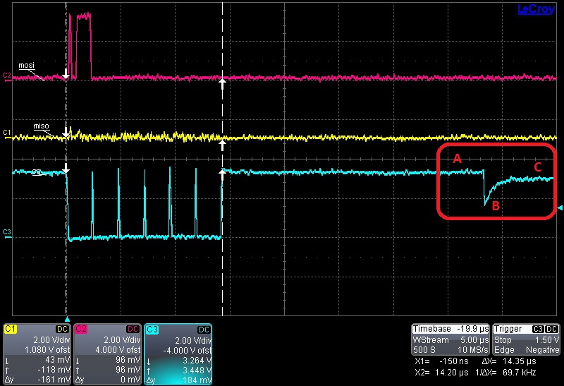
On the right side of the picture position A marks the active output in idle high level state. At position B PIN_remove() is called which invokes PINCC26XX_setIoCfg() which first sets the output value to the default PIN_GPIO_LOW causing the glitch and than shortly after the output buffer is disabled which lets the IO line float high at position C due to the external pull-up resistor present.


To avoid the issue PINCC26XX_setIoCfg() shall check whether the output buffer is active or disabled.

  • If the output buffer is disabled the API shall set the output level first to avoid switch-on glitches.
  • If the output driver is enabled it shall disable the output buffer first and shall set the output level only afterwards.

Please fix the above described issue and if possible provide information on whether the bug can be fixed in the next TI-RTOS for CC13xx and CC26xx release and whether the fix would make it into the next CC26xx BLE-SDK release.

Thank you in advance for your kind support.

Best regards,

 Tamas

_

  • I have asked someone in the CC26xx drivers team to look into this.

    Alan
  • Hello Alan,

    the following code example implements the proposal from the above issue report.

    // Internal utility function for setting IOCFG register for pin
    static void PINCC26XX_setIoCfg(PIN_Config bmMask, PIN_Config pinCfg) {
        uint32_t dsCfg;
        PIN_Id pinId = PIN_ID(pinCfg);
        bool bInvChanges;
    
        if (pinCfg&PIN_GEN) {
            // Translate from device-independent to device-specific PIN_Config values
            pinCfg ^= PIN_GEN|PIN_BM_INPUT_EN|PIN_BM_PULLING;
        }
        // Get existing IOCFG, determine whether inversion changes, mask away what will be updated
        dsCfg = HWREG(IOC_BASE+IOC_O_IOCFG0+4*pinId);
        bInvChanges = (dsCfg^pinCfg)&bmMask&PINCC26XX_INV_INOUT;
        dsCfg &= ~bmMask;
    
        // Insert what we want to update, possibly revert IRQ edges, write back to IOCFG
        dsCfg |= (pinCfg&bmMask&PINCC26XX_BM_IOCFG);
        if ((bmMask&PINCC26XX_BM_IRQ)==PINCC26XX_BM_IRQ && (dsCfg&PINCC26XX_INV_INOUT)==0) {
            // We're changing IRQ options but inversion will not be enabled -> keep IRQ options
        } else if ((bmMask&PINCC26XX_BM_IRQ)==0 && !bInvChanges) {
            // We're not changing IRQ options and inversion remains unchanged -> keep IRQ options
        } else {
            // We're updating IRQ options and inversion will be enabled, OR
            // we're not updating IRQ options but inversion settings change
            // -> reverse polarity of edge detection when positive-only or negative-only
            switch (dsCfg&PINCC26XX_BM_IRQ) {
            case PINCC26XX_IRQ_POSEDGE:
                dsCfg &= ~PINCC26XX_BM_IRQ;
                dsCfg |= PINCC26XX_IRQ_NEGEDGE;
                break;
            case PINCC26XX_IRQ_NEGEDGE:
                dsCfg &= ~PINCC26XX_BM_IRQ;
                dsCfg |= PINCC26XX_IRQ_POSEDGE;
                break;
            default:
                break;
            }
        }
        HWREG(IOC_BASE+IOC_O_IOCFG0+4*pinId) = dsCfg;
    
        // Update GPIO output value and enable depending on previous output mode (enabled or disabled)
        {
            bool bOutputEnabled = (HWREG(GPIO_BASE+GPIO_O_DOE31_0)&(1<<pinId)) ? true : false;
    
            if(!bOutputEnabled) {
                if (bmMask&PINCC26XX_BM_GPIO_OUTPUT_VAL) {
                    // Set GPIO output value
                    HWREGB(GPIO_BASE+GPIO_O_DOUT3_0+pinId) = (pinCfg&PINCC26XX_BM_GPIO_OUTPUT_VAL) ? 1 : 0;
                }
            }
    
            if (bmMask&PINCC26XX_BM_GPIO_OUTPUT_EN) {
                // Set GPIO output enable
                uint32_t key = Hwi_disable();
                    HWREG(GPIO_BASE+GPIO_O_DOE31_0) =
                        (HWREG(GPIO_BASE+GPIO_O_DOE31_0) & ~(1<<pinId)) |
                        ((pinCfg&PINCC26XX_BM_GPIO_OUTPUT_EN) ? (1<<pinId) : 0);
                Hwi_restore(key);
            }
    
            if(bOutputEnabled) {
                if (bmMask&PINCC26XX_BM_GPIO_OUTPUT_VAL) {
                    // Set GPIO output value
                    HWREGB(GPIO_BASE+GPIO_O_DOUT3_0+pinId) = (pinCfg&PINCC26XX_BM_GPIO_OUTPUT_VAL) ? 1 : 0;
                }
            }
        }
    }

    Unfortunately it turned out that this change does not remove the spike entirely. Based on further investigations it seems that the glitch on the output is partly caused by the event of detaching the given IO pin from the SSI peripheral mux reverting it back to GPIO mux mode which is supposed to be in high impedance tri-state at that time with the external pull-up device weakly pulling the line up.

    The following code snippet is from PIN_remove():

            // Find GPIO default value and revert to it
            if (PinGpioConfigTable[pinId]==PIN_UNASSIGNED) {
                // Revert pin to default configuration:
                // GPIO, input buffer disable, GPIO output disable, low GPIO output, no pull, no IRQ, no wakeup
                PINCC26XX_setIoCfg(PIN_BM_ALL, PIN_ID(pinId)|PIN_INPUT_DIS);
            } else {
                // Revert pin to previous GPIO configuration
                PINCC26XX_setIoCfg(PIN_BM_ALL, pPinGpio[PinGpioConfigTable[pinId]]);
            }
            // Revert to GPIO
            PINCC26XX_setIoCfgMux(PIN_ID(pinId), -1);

    First the GPIO is reconfigured to be in tri-state mode and finally the SSI mux of the pin is reverted to GPIO mode effectively releasing the pin and letting the external pull-up device to drive the line.

    To minimize the glitch on the output when the mux is changed I had to change the default pin settings to be push-pull output with 2 mA drive strength. This way the glitch is still present but it is only a few hundred millivolts in worst case with a 3V3 VDDS supply which shall not be detected as valid state transition by the external peripherals. Still, from power consumption point of view this is far from ideal.

    Could you please ask the designer team to look into this issue further?

    Thank you for your continued support.

    Best regards,

     Tamas

    _

  • Tamas,

    This thread and the other two are still being reviewed.

    Todd