This thread has been locked.

If you have a related question, please click the "Ask a related question" button in the top right corner. The newly created question will be automatically linked to this question.

C6748 initialising DDR2/mDDR memory controller

Hi,

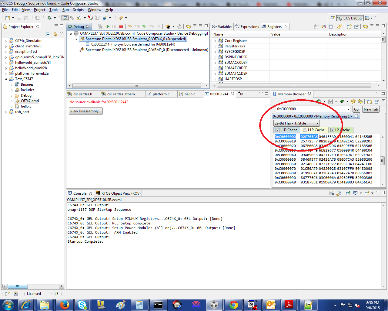
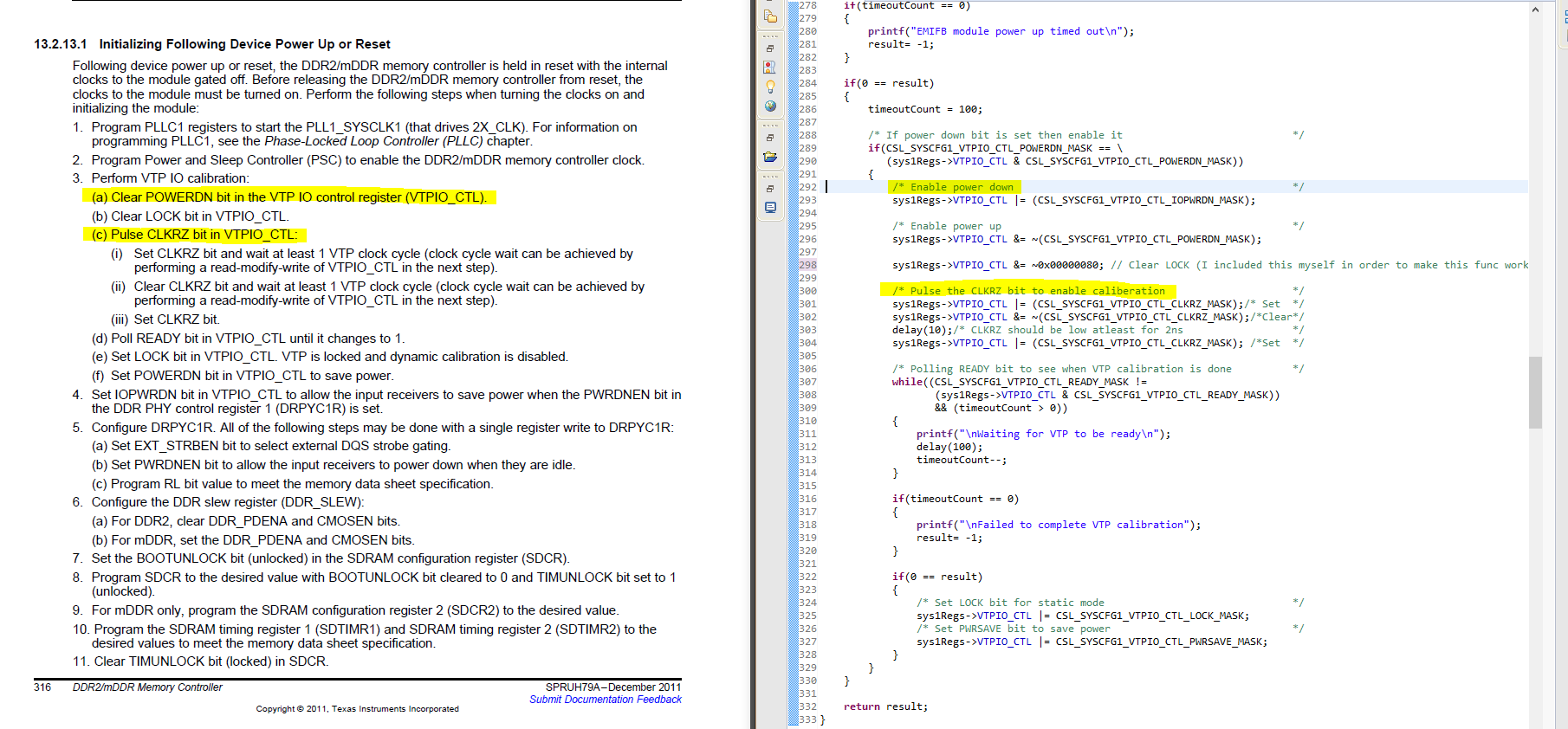
I am trying to configure the DDR2/mDDR memory controller and I am currently following the steps to initialise the module in section 13.2.13.1 of the technical reference. I am also using the example in the cslr for guidance. I realise that the registers provided in the cslr do not match the ones in my watch list as shown in the picture below.

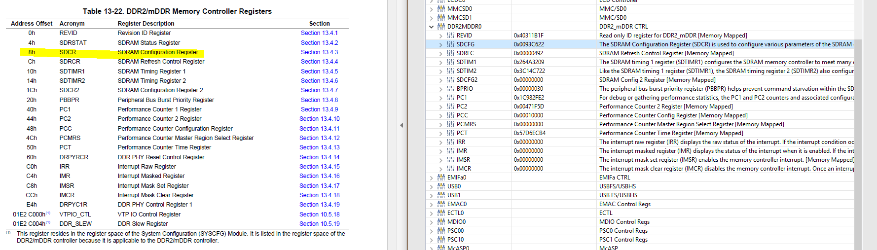
While the register description matches, the names of the registers provided do not have the same name as the one in my watch list, furthermore it seems that some of the registers listed in the technical reference manual are missing. Is there a known solution to solve this? Thank you.

Regards,
Jerome Lieow

  • Dear Jerome Lieow,

    If you feel any difference, you can use "Memory browser" to dump the register values.

    You can refer gel file for DDR initialization code.

  • Hi Jerome Lieow,

    SDCFG is nothing but the SDCR. What you see and refer in the CCS window is the "SDRAM configuration register". Infact in the CCS window,check next to the "value" field

    i.e., the description field says that as "SDCFG    0x00134832    The SDRAM Configuration Register (SDCR) is used to configure various parameters of the SDRAM..."

    I hope this clarifies!.

  • Hi Shankari,

    I do realise that the register descriptor match, but the registers available in the watch list is incomplete and does not include the DRPYC1R register. This register needs to be configured in order to initialise the DDR2 module.

    Regards,
    Jerome Lieow
  • Hi Titus,

    Thank you, that works and I can adjust values as needed. However I am a bit concerned about the way the DDR2 is initialised. I am following the example in the technical reference under section 13.2.13.1 and using the evm6748 csl mddr example as a guide. In the example file provided, some of the steps differ from the technical reference. For example, for VTP IO calibration, the csl example provided enables power down, enables the IOPOWERDN and POWERDN bit instead of clearing the POWERDN and LOCK bit which I had to add in myself as I commented.

    Is the example provided in the CSL wrong or am I missing something here? 

    Regards,
    Jerome Lieow

  • Hi Jerome,

    It is always recommended to follow the technical reference manual. But on the other hand, as long as the CSL program initilaises the DDR2

    memory without any problem, you can consider avoiding too. Sometimes the example programs may not strictly cover everything stated in the manual.

    As well, check the date of the release of CSL package versus the revision number and date of the Technical reference manual.

  • Hi Shankari,

    I took your advice and followed the technical reference manual instead and found everything to be working. Thank you.

    Regards,
    Jerome Lieow
  • Hi Jerome,

    Thanks for closing the post.

    You are welcome!.