This thread has been locked.

If you have a related question, please click the "Ask a related question" button in the top right corner. The newly created question will be automatically linked to this question.

SPI1 Clock C6748

Other Parts Discussed in Thread: OMAPL138, SYSBIOS

Hi all,

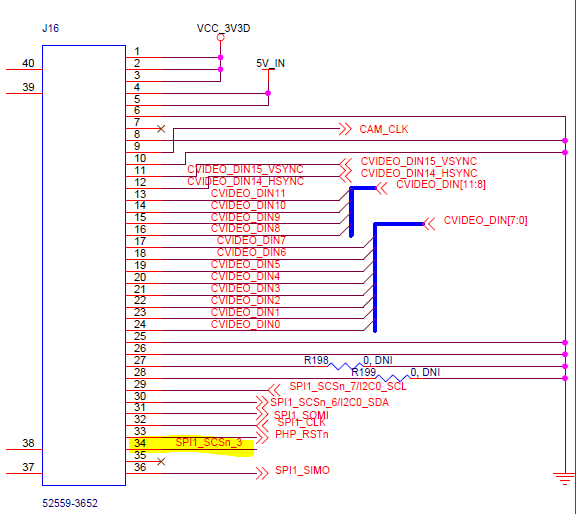
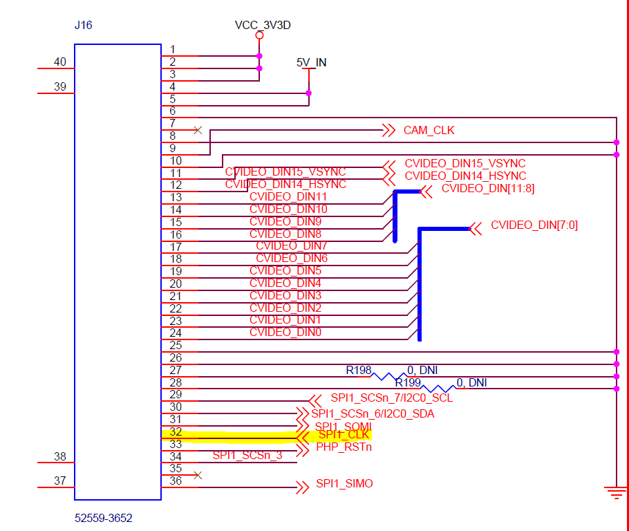
I am trying to configure the SPI1 for use however when I place the line on a probe I cannot see the SPI1's clock signal. I connected the probe to the zif connector's pin 32 output as shown in the picture below. (Highlighted pin is the one currently being probed).


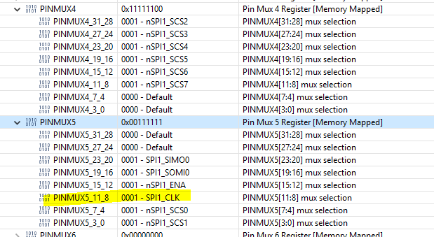
I have set up the SPIGCR1.clkmod register to be 1 (internal clock), and set the SPIPC0.CLKFUN to be 1 (SPI function pin) as well. I know that the SPI1 uses the ASYNC3 clock as its source and by default the ASYNC3 uses the PLL0_SYSCLK2 by default. The GEL file for the C6748 initialises the PLL0 for 300MHz. I have followed the technical reference step by step and I do not know what else is needed or am I missing something. In my understanding, the SPI1 clock should run once I have set the pin to be an SPI function pin. Is there anyone who has experienced this problem?

Regards,
Jerome Lieow

  • Dear Jerome,
    Have you done the PINMUX for SPI1 clock pin ?
    You have to change the PINMUX5 register for SP1_CLK pin.
    PINMUX5_11_8

    Please refer to the OMPL138 TRM guide, SYSCFG module chapter.

  • Hi Titus,

    I have set the PINMUX registers as,

    PINMUX3 = 0x11111111;
    PINMUX4 = 0x11111111;
    PINMUX5 = 0x00111111;

    This is for both SPI1 and SPI0 when I was first testing out the SPI0. However even with only the SPI1 enabled it does not have any conflicts and comes out to be,

    PINMUX4 = 0x11111100;
    PINMUX5 = 0x00111111;

    I do not understand what is PINMUX5_11_8 though, does that refer to PINMUX 11 and 8 as well?

    Regards,
    Jerome Lieow
  • Hi Titus,

    I think it is also worth mentioning that I wrote this to enable the SPI1 module

    CSL_FINS(psc1Regs->MDCTL[CSL_PSC_SPI1], PSC_MDCTL_NEXT, 0x3); //Changes the next state of the SPI1 to the enable state
    CSL_FINS(psc1Regs->PTCMD, PSC_PTCMD_GO0, 0x1); //Write of 1 causes PSC to transition to any new NEXT state

    Seeing as the SPI1 module's power domain is PD0, GO[0] should be the correct bit to cause the PSC transition.

    Regards,
    Jerome Lieow
  • Hi Titus,

    I did some digging and found this post "e2e.ti.com/.../291379". Someone mentioned that the SPICLK signal is only on during data transmission, is this correct? Thank you.

    Regards,
    Jerome Lieow
  • Dear Jerome,

    Yes, you can see the clocks when SPI is transfer (CS active) the data like I2C.

    Try to run the following SPI code on your board and see the signal transitions on SPI.

    C:\ti\OMAPL138_StarterWare_1_10_04_01\build\c674x\cgt_ccs\omapl138\lcdkOMAPL138\spi

    C:\ti\OMAPL138_StarterWare_1_10_04_01\examples\lcdkOMAPL138\spi

    1) You need to enable the SPI PSC module.

    2) You need to enable the PINMUX for the SPI device including CS.

    3) Select SPI transfer mode.

    I do not understand what is PINMUX5_11_8 though, does that refer to PINMUX 11 and 8 as well?

    Its PINMUX5 register and 8-11 is the bit for SPI_CLK pin.

    Please refer to the OMAPL138/C6748 SYSCFG module.

  • Hi Titus,

    I have done all those and my PINMUX5_11_8 is set correctly. I have attached a picture showing that below.

    I have also checked the PDSTAT0 register for the SPI1 to see if the state has changed and it has. 

    I am at my wits end and have no idea what could be wrong except that it might be a hardware issue. I have attached my code below for reference, if you have time can you spot any initialization step that I may have forgotten? Thank you

    Regards,
    Jerome Lieow

    * ======== main.c ========
    */

    #include <xdc/std.h>

    #include <xdc/runtime/Error.h>
    #include <xdc/runtime/System.h>

    #include <ti/sysbios/BIOS.h>

    #include <ti/sysbios/knl/Task.h>

    /*
    * ======== header files for cslr ========
    */

    #include <stdio.h>
    #include <c6x.h>
    #include <cslr/cslr_dspintc.h>
    #include <cslr/soc_C6748.h>
    #include <cslr/cslr_gpio.h>
    #include <cslr/cslr_syscfg0_C6748.h>
    #include <cslr/cslr_psc_C6748.h>


    #include <cslr/cslr_edma3cc.h>
    #include <cslr/cslr_edma3tc.h>
    #include <cslr/cslr_ecap.h>
    #include <cslr/cslr_ehrpwm.h>
    #include <cslr/cslr_cache.h>
    #include <cslr/cslr_vpif.h>
    #include <cslr/cslr_spi.h>
    #include <cslr/cslr_pllc_C6748.h>

    // ============================== INCLUDES =====================================
    //#include "main.h" // contains BUFFSIZE, PSET_EDMA and externs for Src/Dst arrays
    //#include "edma.h" // includes prototypes for all edma functions
    //#include <edma3_drv.h> // LLD Driver header file
    //#include <bios6_edma3_drv_sample.h> // OS-specific and device-specific header file

    /*============================================================================*/
    /* GLOBAL VARIABLES */
    /*============================================================================*/
    //GPIO CONFIG EXAMPLES
    /* sys config registers overlay */
    CSL_SyscfgRegsOvly sysRegs = (CSL_SyscfgRegsOvly)(CSL_SYSCFG_0_REGS);
    /* Psc1 register overlay */
    CSL_PscRegsOvly psc1Regs = (CSL_PscRegsOvly)(CSL_PSC_1_REGS);
    /* Psc0 register overlay */
    CSL_PscRegsOvly psc0Regs = (CSL_PscRegsOvly)(CSL_PSC_0_REGS);
    /* Gpio register overlay */
    CSL_GpioRegsOvly gpioRegs = (CSL_GpioRegsOvly)(CSL_GPIO_0_REGS);
    /* Interrupt Controller Register Overlay */
    CSL_DspintcRegsOvly intcRegs = (CSL_DspintcRegsOvly)CSL_INTC_0_REGS;

    /* EDMA3CC Register Overlay */
    CSL_Edma3ccRegsOvly edma3ccRegs = (CSL_Edma3ccRegsOvly)(CSL_EDMA30CC_0_REGS);

    /* EDMA3CC Register Overlay */
    CSL_Edma3tcRegsOvly edma3tcRegs = (CSL_Edma3tcRegsOvly)(CSL_EDMA30TC_0_REGS );

    /* ecap1 Register Overlay */
    CSL_EcapRegsOvly ecap1Regs = (CSL_EcapRegsOvly)(CSL_ECAP_1_REGS);

    /* ecap2 Register Overlay */
    CSL_EcapRegsOvly ecap2Regs = (CSL_EcapRegsOvly)(CSL_ECAP_2_REGS);

    /* EHRPWM Register Overlay */
    CSL_EhrpwmRegsOvly ehrpwm1Regs = (CSL_EhrpwmRegsOvly)(CSL_EHRPWM_1_REGS);

    /* Cache Register Overlay */
    CSL_CacheRegsOvly CacheRegs = (CSL_CacheRegsOvly)(CSL_MEMPROT_L2_REGS);

    /* VPIF Display Register Overlay */
    CSL_VpifDisRegsOvly vpifDispRegs = (CSL_VpifDisRegsOvly)(CSL_VPIF_0_REGS);

    /* VPIF Capture Register Overlay */
    CSL_VpifCapRegsOvly vpifCapRegs = (CSL_VpifCapRegsOvly)(CSL_VPIF_0_REGS);

    /* VPIF Register Overlay */
    CSL_VpifRegsOvly vpifRegs = (CSL_VpifRegsOvly)(CSL_VPIF_0_REGS);

    /* SPI Register Overlay */
    CSL_SpiRegsOvly spiRegs = (CSL_SpiRegsOvly)(CSL_SPI_1_REGS);

    /* PLL Register Overlay */
    CSL_PllcRegsOvly pll0Regs = (CSL_PllcRegsOvly) CSL_PLLC_0_REGS;

    void main (void)
    {


    //sysRegs->PINMUX3 = 0x11111111; //PINMUX for SPI1
    sysRegs->PINMUX4 = 0x11111100; //PINMUX for SPI1
    sysRegs->PINMUX5 = 0x00111111;

    //Set SPI0 and SPI1 to Enable state
    //CSL_FINS(psc0Regs->MDCTL[CSL_PSC_SPI0], PSC_MDCTL_NEXT, 0x3); //Changes the next state of the VPIF to the enable state
    CSL_FINS(psc1Regs->MDCTL[CSL_PSC_SPI1], PSC_MDCTL_NEXT, 0x3); //Changes the next state of the VPIF to the enable state
    psc0Regs->PTCMD = 0x00000003;
    psc1Regs->PTCMD = 0x00000003;

    while(psc0Regs->PTSTAT) // Wait for any pending transitions to complete
    {
    }
    while(psc1Regs->PTSTAT) // Wait for any pending transitions to complete
    {
    }

    //SPI register settings for 4pin and Chip Select
    CSL_FINS(spiRegs->SPIGCR0, SPI_SPIGCR0_RESET, 0x0); //Resets SPI
    CSL_FINS(spiRegs->SPIGCR0, SPI_SPIGCR0_RESET, 0x1); //Takes SPI out of reset
    CSL_FINS(spiRegs->SPIGCR1, SPI_SPIGCR1_ENABLE, 0x1); //Enables SPI Communication
    CSL_FINS(spiRegs->SPIGCR1, SPI_SPIGCR1_LOOPBACK, 0x0); //Disables internal loopback
    CSL_FINS(spiRegs->SPIGCR1, SPI_SPIGCR1_POWERDOWN, 0x0); //Disables power-down mode. Setting this bit stops the clocks to the SPI internal logic and the SPI registers.
    CSL_FINS(spiRegs->SPIGCR1, SPI_SPIGCR1_CLKMOD, 0x1); //Sets SPIx_CLK as an o/p
    CSL_FINS(spiRegs->SPIGCR1, SPI_SPIGCR1_MASTER, 0x1); //Sets SPI as Master
    CSL_FINS(spiRegs->SPIPC0, SPI_SPIPC0_SOMIFUN, 0x1); //Sets MISO pin as SPI function pin
    CSL_FINS(spiRegs->SPIPC0, SPI_SPIPC0_SIMOFUN, 0x1); //Sets MOSI pin as SPI function pin
    CSL_FINS(spiRegs->SPIPC0, SPI_SPIPC0_CLKFUN, 0x1); //Sets SPICLK pin as SPI function pin
    CSL_FINS(spiRegs->SPIPC0, SPI_SPIPC0_ENAFUN, 0x0); //Disables ENAFUN pin
    CSL_FINS(spiRegs->SPIPC0, SPI_SPIPC0_SCS0FUN7, 0x0);
    CSL_FINS(spiRegs->SPIPC0, SPI_SPIPC0_SCS0FUN6, 0x0);
    CSL_FINS(spiRegs->SPIPC0, SPI_SPIPC0_SCS0FUN5, 0x0);
    CSL_FINS(spiRegs->SPIPC0, SPI_SPIPC0_SCS0FUN4, 0x0);
    CSL_FINS(spiRegs->SPIPC0, SPI_SPIPC0_SCS0FUN3, 0x0); //SCSn1 is used
    CSL_FINS(spiRegs->SPIPC0, SPI_SPIPC0_SCS0FUN2, 0x0);
    CSL_FINS(spiRegs->SPIPC0, SPI_SPIPC0_SCS0FUN1, 0x1);
    CSL_FINS(spiRegs->SPIPC0, SPI_SPIPC0_SCS0FUN0, 0x0);

    //Configuring SPIDAT1 to use SPIFMT0
    CSL_FINS(spiRegs->SPIDAT1, SPI_SPIDAT1_DFSEL, 0x0); //Choose Data Word Format 0 (SPIFMT0)

    //Sets SPIFMT0
    CSL_FINS(spiRegs->SPIFMT[0], SPI_SPIFMT_WDELAY, 0x2); //Delay between transmission is WDELAY x (Period of SPI CLK) + 2 x (Period of SPI CLK)
    CSL_FINS(spiRegs->SPIFMT[0], SPI_SPIFMT_PARPOL, 0x0); //0 for even parity flag, 1 for odd parity flag; added at the end of the transmit data stream
    CSL_FINS(spiRegs->SPIFMT[0], SPI_SPIFMT_PARENA, 0x0); //Parity enable. 0 to disable, 1 to generate parity bit at the end of transmit data stream
    CSL_FINS(spiRegs->SPIFMT[0], SPI_SPIFMT_WAITENA, 0x0); //The SPI does not wait for the SPIx_ENA signal from the slave and starts the transfer
    CSL_FINS(spiRegs->SPIFMT[0], SPI_SPIFMT_SHIFTDIR, 0x1); //1 for MSB to shift out first, 0 for LSB to shift out first
    CSL_FINS(spiRegs->SPIFMT[0], SPI_SPIFMT_DISCSTIMERS, 0x1); //No C2TDELAY or T2CDELAY is inserted in the chip select timings
    CSL_FINS(spiRegs->SPIFMT[0], SPI_SPIFMT_POLARITY, 0x0); //SPI clk sig is low-inactive (before and after data transfer the clock signal is low)
    CSL_FINS(spiRegs->SPIFMT[0], SPI_SPIFMT_PHASE, 0x0); //SPI clock signal is not delayed versus the transmit/receive data stream
    CSL_FINS(spiRegs->SPIFMT[0], SPI_SPIFMT_PRESCALE, 0x2);
    CSL_FINS(spiRegs->SPIFMT[0], SPI_SPIFMT_CHARLEN, 0x10);

    // //Sets SPIDELAY (Shouldnt be needed)
    // CSL_FINS(spiRegs->SPIDELAY, SPI_SPIDELAY_C2TDELAY, 0x2); //Defines a setup time for the slave device that delays the data transmission from the chip select active edge
    // CSL_FINS(spiRegs->SPIDELAY, SPI_SPIDELAY_T2CDELAY, 0x2); //Defines a hold time for the slave device that delays the chip select deactivation
    // CSL_FINS(spiRegs->SPIDELAY, SPI_SPIDELAY_T2EDELAY, 0x0); //Defines a time-out value as a multiple of SPI clock before the SPIx_ENA signal has to become inactive and after the CS becomes inactive
    // CSL_FINS(spiRegs->SPIDELAY, SPI_SPIDELAY_C2EDELAY, 0x0); //defines the maximum time between the SPI activates the chip select signal and the addressed slave has to respond by activating the SPIx_ENA signal

    spiwrite();

    }

    void spiwrite(){


    spiRegs->SPIDEF = 0b11111111; //Asserting all Chip Select pins
    spiRegs->SPIDEF = 0b11111101; //Deasserting Chip Select 1 pin, write start

    spiRegs->SPIDAT0 = 0xFF;

    spiRegs->SPIDEF = 0b11111111; //Asserting all Chip Select pins, write end


    }


  • It seems you are working with C6748 or OMAPL138 LCDK board, right ?
    Let me try the same on my board and update you.

    BTW, I'm going to use the following examples.
    C:\ti\OMAPL138_StarterWare_1_10_04_01\build\c674x\cgt_ccs\omapl138\lcdkOMAPL138\spi
    C:\ti\pdk_OMAPL138_1_01_00_02\packages\ti\csl\exampleProjects\spi_exampleProject
  • Hi Titus,

    Thanks for your help, and I await your update. I am also unable to toggle SPI1's chip select 3 pin and see a response on pin 34.

    I know I am writing to the right registers because I am able to toggle chip selects 6 and 7 on pin 30 and 29 and chip selects 1 and 0 available on the expansion header. 

    Regards,
    Jerome Lieow


  • I am also unable to toggle SPI1's chip select 3 pin and see a response on pin 34.

    Please try to probe in R208 and R209 (try both ends of resistor)

    You have to short the R208 to get the SPI1_nCS3 pin on J16 connector.
  • Hi Titus,

    Thank you, I am now able to see a response from chip select 3 on the zif. Are you able to see SPI1_clk signal on the zif though? I am only able to see the SPI1_clk signal when I stop the program I am running on the board. I suspect that means that the SPI1_clk signal is effectively being pulled to some state within the board itself rendering SPI1 unusable. Could you confirm this?

    Regards,
    Jerome Lieow

  • Hi Titus,

    The clock of SPI1 can now be seen when I set GPIO2 as an output. Thank you for your help with the hardware config, without it, I would be stuck for a long time.

    Regards,
    Jerome Lieow
  • Dear Jerome,
    Glad to hear that you able to solve the problem.
    Thanks for the update.