Hi Forum,
I am currently developing a gpmc bus with 4 chip select memory mapped regions.
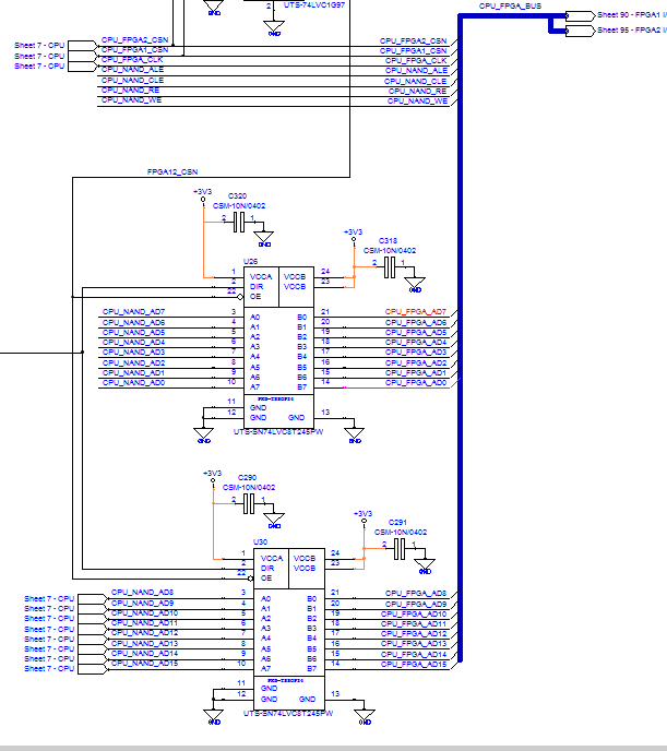
the nand bus width is 16
cs1 -> is a 8 bit (ad0-ad7)
cs3 ->is a 8 bit (ad0-ad7)
cs5->is a 16bit(ad0-ad15)
cs6->is a 16 bit(ad0-ad15)
below is my device tree settings for nand
	nand_flash_x8_default: nand_flash_x8_default {
 	pinctrl-single,pins = <

		0x3c ( PIN_INPUT_PULLUP | MUX_MODE0 ) /* (A11) gpmc_ad15.gpmc_ad15 */
		0x38 ( PIN_INPUT_PULLUP | MUX_MODE0 ) /* (B11) gpmc_ad14.gpmc_ad14 */
		0x34 ( PIN_INPUT_PULLUP | MUX_MODE0 ) /* (C11) gpmc_ad13.gpmc_ad13 */
		0x30 ( PIN_INPUT_PULLUP | MUX_MODE0 ) /* (E11) gpmc_ad12.gpmc_ad12 */
		0x2c ( PIN_INPUT_PULLUP | MUX_MODE0 ) /* (D11) gpmc_ad11.gpmc_ad11 */
		0x28 ( PIN_INPUT_PULLUP | MUX_MODE0 ) /* (F11) gpmc_ad10.gpmc_ad10 */
		0x24 ( PIN_INPUT_PULLUP | MUX_MODE0 ) /* (A10) gpmc_ad9.gpmc_ad9 */
		0x20 ( PIN_INPUT_PULLUP | MUX_MODE0 ) /* (B10) gpmc_ad8.gpmc_ad8 */
		0x1c ( PIN_INPUT_PULLUP | MUX_MODE0 ) /* (B8) gpmc_ad7.gpmc_ad7 */
		0x18 ( PIN_INPUT_PULLUP | MUX_MODE0 ) /* (C8) gpmc_ad6.gpmc_ad6 */
		0x14 ( PIN_INPUT_PULLUP | MUX_MODE0 ) /* (A7) gpmc_ad5.gpmc_ad5 */
		0x10 ( PIN_INPUT_PULLUP | MUX_MODE0 ) /* (B7) gpmc_ad4.gpmc_ad4 */
		0xc  ( PIN_INPUT_PULLUP | MUX_MODE0 ) /* (A6) gpmc_ad3.gpmc_ad3 */
		0x8  ( PIN_INPUT_PULLUP | MUX_MODE0 ) /* (B6) gpmc_ad2.gpmc_ad2 */
		0x4  ( PIN_INPUT_PULLUP | MUX_MODE0 ) /* (A5) gpmc_ad1.gpmc_ad1 */
		0x0  ( PIN_INPUT_PULLUP | MUX_MODE0 ) /* (B5) gpmc_ad0.gpmc_ad0 */
		0x70 ( PIN_INPUT_PULLUP | MUX_MODE0 ) /* (A2) gpmc_wait0.gpmc_wait0 */
		0x8c ( PIN_INPUT_PULLUP | MUX_MODE2 ) /* (A12) gpmc_clk.gpmc_wait1 */
		0x7c ( PIN_OUTPUT | MUX_MODE0 ) /* (A8) gpmc_csn0.gpmc_csn0 */
		0x88 ( PIN_OUTPUT | MUX_MODE0 ) /* (B12) gpmc_csn3.gpmc_csn3 */
		0x74 ( PIN_OUTPUT | MUX_MODE2 ) /* (B3) gpmc_wpn.gpmc_csn5 */
		0x78 ( PIN_OUTPUT | MUX_MODE2 ) /* (A3) gpmc_be1n.gpmc_csn6 */
		0x90 ( PIN_OUTPUT | MUX_MODE0 ) /* (A9) gpmc_advn_ale.gpmc_advn_ale */
		0x94 ( PIN_OUTPUT | MUX_MODE0 ) /* (E10) gpmc_oen_ren.gpmc_oen_ren */
		0x98 ( PIN_OUTPUT | MUX_MODE0 ) /* (D10) gpmc_wen.gpmc_wen */
		0x9c ( PIN_OUTPUT | MUX_MODE0 ) /* (C10) gpmc_be0n_cle.gpmc_be0n_cle */


		>;
	};
&gpmc {
	status = "okay"; /* Disable eMMC when enabling GPMC/NAND */
	pinctrl-names = "default", "sleep";
	pinctrl-0 = <&nand_flash_x8_default>;
	pinctrl-1 = <&nand_flash_x8_sleep>;
        gpmc,num-cs = <7>;
	ranges = <0 0 0x01000000 0x010000000	/* minimum GPMC partition = 16MB */
		  3 0 0x03000000 0x10000000
		  5 0 0x05000000 0x10000000
                  6 0 0x07000000 0x10000000>;
	nand@0,0 {
		reg = <0 0 0x01000000>;		/* device IO registers */
		ti,nand-ecc-opt = "bch16";
		ti,elm-id = <&elm>;
		nand-bus-width = <16>;
		gpmc,device-width = <1>;
		gpmc,sync-clk-ps = <0>;
		gpmc,cs-on-ns = <0>;
		gpmc,cs-rd-off-ns = <40>;
		gpmc,cs-wr-off-ns = <40>;
		gpmc,adv-on-ns = <0>;
		gpmc,adv-rd-off-ns = <25>;
		gpmc,adv-wr-off-ns = <25>;
		gpmc,we-on-ns = <0>;
		gpmc,we-off-ns = <20>;
		gpmc,oe-on-ns = <3>;
		gpmc,oe-off-ns = <30>;
		gpmc,access-ns = <30>;
		gpmc,rd-cycle-ns = <40>;
		gpmc,wr-cycle-ns = <40>;
		gpmc,wait-pin = <0>;
		gpmc,bus-turnaround-ns = <0>;
		gpmc,cycle2cycle-delay-ns = <0>;
		gpmc,clk-activation-ns = <0>;
		gpmc,wait-monitoring-ns = <0>;
		gpmc,wr-access-ns = <40>;
		gpmc,wr-data-mux-bus-ns = <0>;
		/* MTD partition table */
		/* All SPL-* partitions are sized to minimal length
		 * which can be independently programmable. For
		 * NAND flash this is equal to size of erase-block */
		#address-cells = <1>;
		#size-cells = <1>;
		partition@0 {
			label = "NAND.SPL";
			reg = <0x00000000 0x00040000>;
		};
		partition@1 {
			label = "NAND.SPL.backup1";
			reg = <0x00040000 0x00040000>;
		};
		partition@2 {
			label = "NAND.SPL.backup2";
			reg = <0x00080000 0x00040000>;
		};
		partition@3 {
			label = "NAND.SPL.backup3";
			reg = <0x000c0000 0x00040000>;
		};
		partition@4 {
			label = "NAND.u-boot-spl-os";
			reg = <0x00100000 0x00080000>;
		};
		partition@5 {
			label = "NAND.u-boot";
			reg = <0x00180000 0x00100000>;
		};
		partition@6 {
			label = "NAND.u-boot-env";
			reg = <0x00280000 0x00040000>;
		};
		partition@7 {
			label = "NAND.u-boot-env.backup1";
			reg = <0x002c0000 0x00040000>;
		};
		partition@8 {
			label = "NAND.kernel";
			reg = <0x00300000 0x00700000>;
		};
		partition@9 {
			label = "NAND.file-system";
			reg = <0x00a00000 0x1f600000>;
		};
	};
	nand@3,0 {
		reg = <3 0 0x01000000>;		/* device IO registers */
		ti,nand-ecc-opt = "bch16";
		ti,elm-id = <&elm>;
		nand-bus-width = <16>;
		gpmc,device-width = <1>;
		gpmc,sync-clk-ps = <0>;
		gpmc,cs-on-ns = <0>;
		gpmc,cs-rd-off-ns = <40>;
		gpmc,cs-wr-off-ns = <40>;
		gpmc,adv-on-ns = <0>;
		gpmc,adv-rd-off-ns = <25>;
		gpmc,adv-wr-off-ns = <25>;
		gpmc,we-on-ns = <0>;
		gpmc,we-off-ns = <20>;
		gpmc,oe-on-ns = <3>;
		gpmc,oe-off-ns = <30>;
		gpmc,access-ns = <30>;
		gpmc,rd-cycle-ns = <40>;
		gpmc,wr-cycle-ns = <40>;
		gpmc,wait-pin = <0>;
		gpmc,bus-turnaround-ns = <0>;
		gpmc,cycle2cycle-delay-ns = <0>;
		gpmc,clk-activation-ns = <0>;
		gpmc,wait-monitoring-ns = <0>;
		gpmc,wr-access-ns = <40>;
		gpmc,wr-data-mux-bus-ns = <0>;
		#address-cells = <2>;
		#size-cells = <1>;
	};
	nand@5,0 {
		reg = <5 0 0x01000000>;		/* device IO registers */
		ti,nand-ecc-opt = "bch16";
		ti,elm-id = <&elm>;
		nand-bus-width = <16>;
		gpmc,device-width = <2>;
		gpmc,sync-clk-ps = <0>;
		gpmc,cs-on-ns = <0>;
		gpmc,cs-rd-off-ns = <40>;
		gpmc,cs-wr-off-ns = <40>;
		gpmc,adv-on-ns = <0>;
		gpmc,adv-rd-off-ns = <25>;
		gpmc,adv-wr-off-ns = <25>;
		gpmc,we-on-ns = <0>;
		gpmc,we-off-ns = <20>;
		gpmc,oe-on-ns = <3>;
		gpmc,oe-off-ns = <30>;
		gpmc,access-ns = <30>;
		gpmc,rd-cycle-ns = <40>;
		gpmc,wr-cycle-ns = <40>;
		gpmc,wait-pin = <0>;
		gpmc,bus-turnaround-ns = <0>;
		gpmc,cycle2cycle-delay-ns = <0>;
		gpmc,clk-activation-ns = <0>;
		gpmc,wait-monitoring-ns = <0>;
		gpmc,wr-access-ns = <40>;
		gpmc,wr-data-mux-bus-ns = <0>;
		#address-cells = <2>;
		#size-cells = <1>;
	};
	nand@6,0 {
		reg = <6 0 0x01000000>;		/* device IO registers */
		ti,nand-ecc-opt = "bch16";
		ti,elm-id = <&elm>;
		nand-bus-width = <16>;
		gpmc,device-width = <2>;
		gpmc,sync-clk-ps = <0>;
		gpmc,cs-on-ns = <0>;
		gpmc,cs-rd-off-ns = <40>;
		gpmc,cs-wr-off-ns = <40>;
		gpmc,adv-on-ns = <0>;
		gpmc,adv-rd-off-ns = <25>;
		gpmc,adv-wr-off-ns = <25>;
		gpmc,we-on-ns = <0>;
		gpmc,we-off-ns = <20>;
		gpmc,oe-on-ns = <3>;
		gpmc,oe-off-ns = <30>;
		gpmc,access-ns = <30>;
		gpmc,rd-cycle-ns = <40>;
		gpmc,wr-cycle-ns = <40>;
		gpmc,wait-pin = <0>;
		gpmc,bus-turnaround-ns = <0>;
		gpmc,cycle2cycle-delay-ns = <0>;
		gpmc,clk-activation-ns = <0>;
		gpmc,wait-monitoring-ns = <0>;
		gpmc,wr-access-ns = <40>;
		gpmc,wr-data-mux-bus-ns = <0>;
		#address-cells = <2>;
		#size-cells = <1>;
	};


};
when i do a devmem2 from my command line on the 8 bits and the 16 bits the outputs are of these types alternating FF00 whilst i am expecting all 00000 upon reset
root@am437x-evm:~# devmem2 0x03000000 b
/dev/mem opened.
Memory mapped at address 0xb6f6a000.
Read at address  0x03000000 (0xb6f6a000): 0x00
root@am437x-evm:~# devmem2 0x05000000 h
/dev/mem opened.
Memory mapped at address 0xb6f3e000.
Read at address  0x05000000 (0xb6f3e000): 0xFF00
root@am437x-evm:~# devmem2 0x07000000 h
/dev/mem opened.
Memory mapped at address 0xb6f20000.
Read at address  0x07000000 (0xb6f20000): 0xFF00
root@am437x-evm:~# devmem2 0x03000000 h
/dev/mem opened.
Memory mapped at address 0xb6fc7000.
Read at address  0x03000000 (0xb6fc7000): 0xFF00
root@am437x-evm:~# devmem2 0x03000000 w
/dev/mem opened.
Memory mapped at address 0xb6f76000.
Read at address  0x03000000 (0xb6f76000): 0xFF00FF00
root@am437x-evm:~#
I would really appreciate if someone could point out what i might be doing wrong here.
-Parker