Other Parts Discussed in Thread: AM4379
Hi,
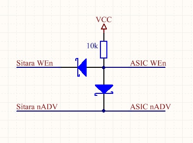
I am currently trying to implement GPMC pus as a parallel interface In my am4379 custom board. I have connected the cs3 to the external asic. the gpmc bus is 16 bits wide and the device is a 8 bit device in address data multiplexed mode. my write enable does not deassert for address write section. I am trying to access the chip in asynchronous single read and write mode. I have memory mapped the peripheral and i could see the chip select pins going low when i try to access that mapped region. below are the timing diagram for the chip i am trying to communicate with. and the device tree settings.
	nand_flash_x8_default: nand_flash_x8_default {
 	pinctrl-single,pins = <

		0x3c ( PIN_INPUT | MUX_MODE0 ) /* (A11) gpmc_ad15.gpmc_ad15 */
		0x38 ( PIN_INPUT | MUX_MODE0 ) /* (B11) gpmc_ad14.gpmc_ad14 */
		0x34 ( PIN_INPUT | MUX_MODE0 ) /* (C11) gpmc_ad13.gpmc_ad13 */
		0x30 ( PIN_INPUT | MUX_MODE0 ) /* (E11) gpmc_ad12.gpmc_ad12 */
		0x2c ( PIN_INPUT | MUX_MODE0 ) /* (D11) gpmc_ad11.gpmc_ad11 */
		0x28 ( PIN_INPUT | MUX_MODE0 ) /* (F11) gpmc_ad10.gpmc_ad10 */
		0x24 ( PIN_INPUT | MUX_MODE0 ) /* (A10) gpmc_ad9.gpmc_ad9 */
		0x20 ( PIN_INPUT | MUX_MODE0 ) /* (B10) gpmc_ad8.gpmc_ad8 */
		0x1c ( PIN_INPUT | MUX_MODE0 ) /* (B8) gpmc_ad7.gpmc_ad7 */
		0x18 ( PIN_INPUT | MUX_MODE0 ) /* (C8) gpmc_ad6.gpmc_ad6 */
		0x14 ( PIN_INPUT | MUX_MODE0 ) /* (A7) gpmc_ad5.gpmc_ad5 */
		0x10 ( PIN_INPUT | MUX_MODE0 ) /* (B7) gpmc_ad4.gpmc_ad4 */
		0xc  ( PIN_INPUT | MUX_MODE0 ) /* (A6) gpmc_ad3.gpmc_ad3 */
		0x8  ( PIN_INPUT | MUX_MODE0 ) /* (B6) gpmc_ad2.gpmc_ad2 */
		0x4  ( PIN_INPUT | MUX_MODE0 ) /* (A5) gpmc_ad1.gpmc_ad1 */
		0x0  ( PIN_INPUT | MUX_MODE0 ) /* (B5) gpmc_ad0.gpmc_ad0 */
		0x70 ( PIN_INPUT| MUX_MODE0 ) /* (A2) gpmc_wait0.gpmc_wait0 */
		0x8c ( PIN_INPUT |INPUT_EN | MUX_MODE2 ) /* (A12) gpmc_clk.gpmc_wait1 */
		0x7c ( PIN_OUTPUT | MUX_MODE0 ) /* (A8) gpmc_csn0.gpmc_csn0 */
		0x88 ( PIN_OUTPUT | MUX_MODE0 ) /* (B12) gpmc_csn3.gpmc_csn3 */
		0x74 ( PIN_OUTPUT | MUX_MODE2 ) /* (B3) gpmc_wpn.gpmc_csn5 */
		0x78 ( PIN_OUTPUT | MUX_MODE2 ) /* (A3) gpmc_be1n.gpmc_csn6 */
		0x90 ( PIN_OUTPUT |MUX_MODE0 ) /* (A9) gpmc_advn_ale.gpmc_advn_ale */
		0x94 ( PIN_OUTPUT | MUX_MODE0 ) /* (E10) gpmc_oen_ren.gpmc_oen_ren */
		0x98 ( PIN_OUTPUT | MUX_MODE0 ) /* (D10) gpmc_wen.gpmc_wen */
		0x9c ( PIN_OUTPUT | MUX_MODE0 ) /* (C10) gpmc_be0n_cle.gpmc_be0n_cle */


		>;
	};
&gpmc {
	status = "okay"; /* Disable eMMC when enabling GPMC/NAND */
	pinctrl-names = "default", "sleep";
	pinctrl-0 = <&nand_flash_x8_default>;
	pinctrl-1 = <&nand_flash_x8_sleep>;
        ranges = <0 0 0x01000000 0x00100000	/* minimum GPMC partition = 16MB */
		  3 0 0x02000000 0x00100000
		  5 0 0x03000000 0x00100000
                  6 0 0x04000000 0x00100000>;
	nor@3,0 {
		reg = <3 0 0x00100000>;
		bank-width = <2>;
		gpmc,async-read;
		gpmc,async-write;
		gpmc,clk-activation-ns = <20>;
		gpmc,burst-length = <16>;
		gpmc,mux-add-data = <2>;
		gpmc,sync-clk-ps = <10000>;
		gpmc,cs-on-ns = <0>;
		gpmc,cs-rd-off-ns = <80>;
		gpmc,cs-wr-off-ns = <80>;
		gpmc,adv-on-ns = <0>;
		gpmc,adv-rd-off-ns = <20>;
		gpmc,adv-wr-off-ns = <20>;
		gpmc,we-on-ns = <30>;
		gpmc,we-off-ns = <40>;
		gpmc,oe-on-ns = <30>;
		gpmc,oe-off-ns = <40>;
		gpmc,page-burst-access-ns = <10>;
		gpmc,access-ns = <50>;
		gpmc,rd-cycle-ns = <60>;
		gpmc,wr-cycle-ns = <60>;
		gpmc,wr-access-ns = <0>;
		gpmc,wr-data-mux-bus-ns = <30>;
		gpmc,bus-turnaround-ns = <10>;
		gpmc,cycle2cycle-samecsen;
		gpmc,cycle2cycle-delay-ns = <10>;


	};
my expected timing diagram for read and write access:


My problem:
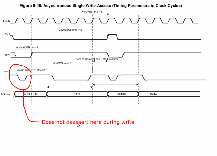

Any suggestions on what i might be doing wrong here? The timing diagrams n the trm for GPMC none of them match to the timings needed to communicate to my chip. Any further advice will be greatly appreciated. Regards
-Parker