


Hi all,
Im working on TCI6638K2K(4ARM+8DSP) Custom Design Board. On my project, all DSP core's exception module is used. I assign adress ranges on DDR3B for all DSP(0x60000000-to-0x80000000). I want to protect these regions to allow every DSP can Read/Write for only own assigned address range. I changed XMC Registers for protection.
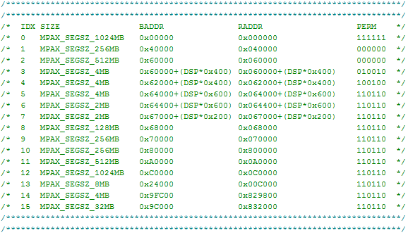
Here is the DDR3B mapping(DSP:0-7);
Here is the DSP1 XMC registers;

Here is the DSP2 XMC registers;

for DSP1, Idx=6 says that, ADDR=0x62400000 mapping to ADDR=0x062400000 and permissions are Readable&Writeable&NotExecutite for next 4MB(Reference Section 7.2.1: sprugw0c.pdf). But DSP1 cannot read&write for this region, exception occured(XMPFAR=0x649A45E0, XMPFSR=0x00000110).
Region 0x64000000-to-0x67000000 is divided 8 part for each DSP has own 6MB. Using MPAX IDX 5&6 for this region(4MB + 2MB).
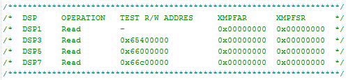
I checked permission of regions for all assigned regions. DSP0,2,4,6 can read/write their own regions and cant read/write another assigned region. But DSP1,3,5,7 failed to read/write their own regions. Last time, i tried adresses below and exception occured, but XMPFAR is zero. What does it mean if XMPFAR&XMPFSR is zero?
Is it something wrong with options?
Thank you,
Best Regards,
Srt


