Because of the Thanksgiving holiday in the U.S., TI E2E™ design support forum responses may be delayed from November 25 through December 2. Thank you for your patience.

This thread has been locked.

If you have a related question, please click the "Ask a related question" button in the top right corner. The newly created question will be automatically linked to this question.

[C5515] data is lost on receive buffer at the begging of I2S frame

Hi,

My customer is now facing the problem with losing I2S data on receive buffer at the begging of I2S frame.

First of all, please take a look at the attached spread sheet. I've tried to explain the phenomenon.
They are in trouble with this issue and need to fix this issue soon.

i2s_issue_report.xlsx

So could you please explain the mechanism for this issue and let us know the related descriptions in the manual you provided.
Also, please review the register configurations (see attached) and let me know if you have any suspicion for this issue.

To me, the register values looks correct and this issue looks I2S clocking issue, I mean some clocks have to be fed to I2S to 'activate' its receive block at the first/beginning of frame sync. This is described in TRM:

1.2.7.2 Receive Path Latency 
After the I2S is enabled, the receive path starts receiving data after: 
• 1 or 2 frame-sync clocks for 8-, 18-, 20-, 24-, or 32-bit data depending on other configuration 
• 1, 2 or 3 frame-sync clocks for 10-, 12-, 14-, or 16-bit data depending on other configuration 
Well, they are using I2S as 16bit word port, so upto 3 frame-syncs might be needed as "dummy" for receiving data.
But as you see in the spread sheet, they are actually loosing 5 frames, not 3. so we need more detailed/additional information for this behavior if the issue is related to this restriction.

Also, the errata might be related to this issue. Please find the following:

www.tij.co.jp/.../sprz308d.pdf
Advisory 2.0.4 I2S: I2S Internal Data Delay

It says 3 zero words reception would be expected at first 3 frames.
But actually DSP does not match this restriction....Also some information is available on Table 6. Feedback Path Internal Data Delays, but in fact, I can't understand what is meant by this table. Could you please explain ?

Anyway, please check the attached spread sheet carefully. I've summarized the issue in detail.
Sorry to have troubled you, but It would be so appreciated if you could reply soon!

Best Regards,
Naoki

  • Hi Naoki-san,

    Would like to check on few obvious things that needs to be taken care. Could you please confirm .

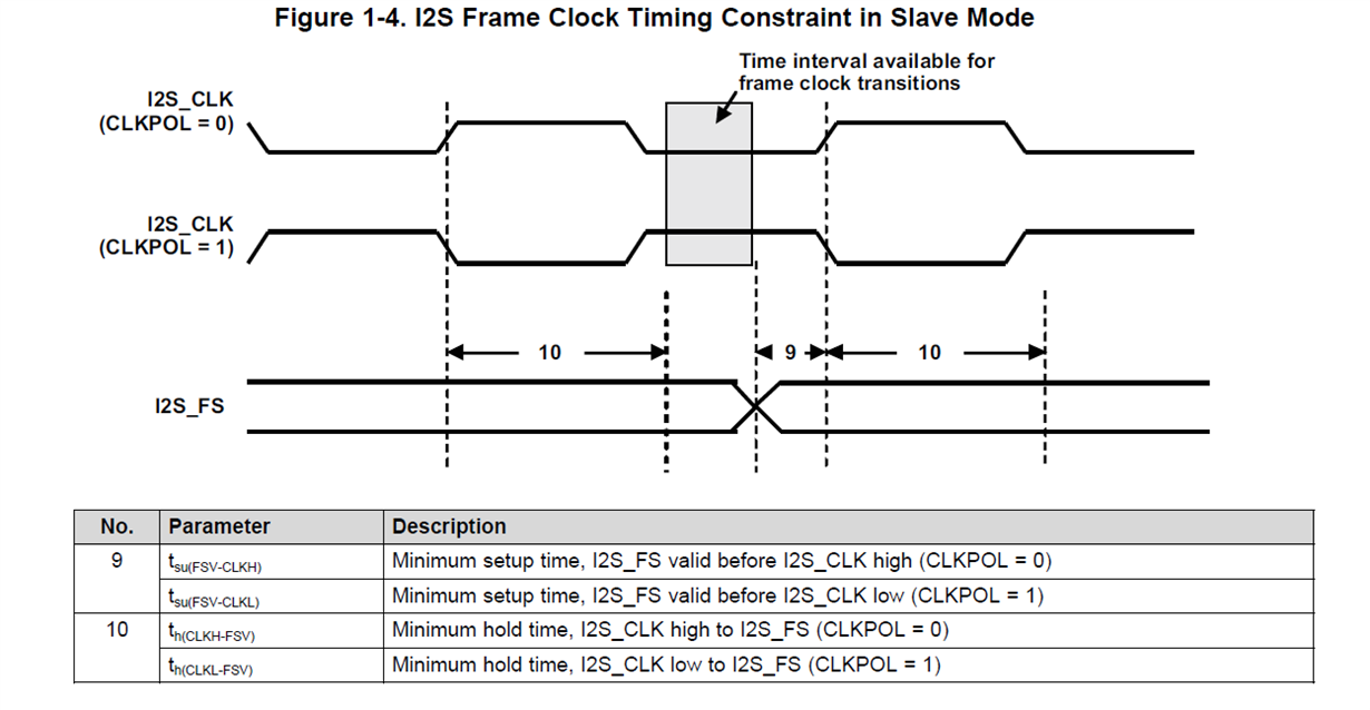
    Since in your case I2S is slave, whether the frame clock timing constraint as mentioned below is met ?


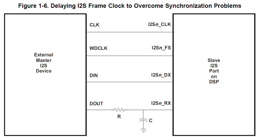
    I believe this is your custom board, if so then whether the following is taken care ? Synchronization issues may occur if the frame clock transitions close to the falling edge of the bit clock violating the previously described hold requirement resulting in incorrect data transfer. In these circumstances, the frame clock should be delayed with respect to the bit clock by introducing a time delay in its signal path as shown in Figure . The RC circuit delays the frame clock by a value given by the relation Trc = RC.


    Parsing through software configuration , it looks ok except for Clock configuration. I2S peripheral clock generator should only be configured if the I2S is configured as a master device. When the I2S is configured as the slave, the external master device supplies the required clocks. Clock Configuration done in the I2S register has no effect when I2S is configured as slave device

    With respect to your question on feedback path :  Feedback path refers to an I2S transmit pin that is externally connected to the I2S receive pin. The table provides the details on delay involved before the actual data is present , the data delay depends on the FSDIV BITS. But I do not think this is applicable for your application.

    Regards

     Vasanth


  • Hi Vasanth,

    Thank you very much for your reply.
    I forwarded the answers to my customer. I'll let you know their feedback later, especially AC timing for frame-sync. So in the meanwhile, please let me ask you some more detail.

    First, I think we need to clarify that their expectation itself is really correct or not, i.e., in their use case, first 3 zero words (coming from errata Advisory 2.0.4) and then 9 0xFFFF words and finally a 0x1555 on receive buffer on the condition they does not violate register configurations and AC timing spec requirements. What do you think of this ?

    Second, I need to confirm the following behavior being described in user guide:
    www.tij.co.jp/.../sprufx4b.pdf
    1.2.7.2 Receive Path Latency
    After the I2S is enabled, the receive path starts receiving data after:
    • 1 or 2 frame-sync clocks for 8-, 18-, 20-, 24-, or 32-bit data depending on other configuration
    • 1, 2 or 3 frame-sync clocks for 10-, 12-, 14-, or 16-bit data depending on other configuration

    What does it actually mean by "1, 2 or 3 frame-sync clocks for 10-, 12-, 14-, or 16-bit data depending on other configuration " ? To me, I feel this implies upto 3 words can be completely lost in their use case. In other words, when using I2S peripheral with slave mode, it starts working (start shifting in Receive Shift Register) just after receiving valid 3 frame-syncs.

    Best Regards,
    Naoki

  • Hi Vasanth,

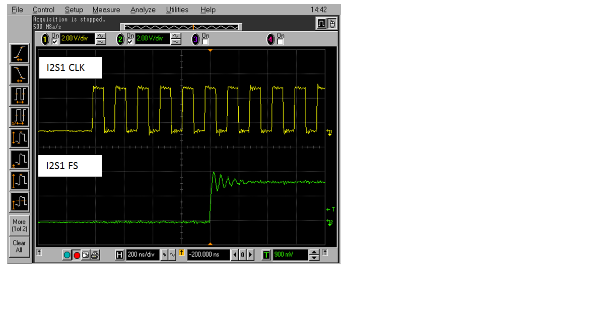
    Some feedback from my customer. The timing margin for frame-sync looks enough. Please find attached. I've added a waveform capture. Also I've updated slightly for the correctness.

    i2s_issue_report_160617.xlsx

    So it looks like missing the incoming 5 frame syncs on I2S peripheral (or DMA) at the very first transfer. Why/How this can happen ?
    Their deadline is almost coming.

    Best Regards,
    Naoki

  • Hi Naoki-san,


    Not sure why the extra padding was done. Could you try not add the extra padding and send the data from Master/Host I2S. In slave mode as per the errata the first 3 bytes received would be zero and needs to be ignored, rest the data needs to look fine..

    Also would suggest to temporarily remove packing and observe the receive data.


    For the above scenarios can you please log the received data and share it with us.


    Regards

    Vasanth

  • Hi Vasanth,

    You meant "extra padding" was the transferred data caused by I2S bus transaction for another device. Correct ?
    In C55x DSP, I2S/DMA was programed to transfer 13 words to its internal memory for the first packet transferred by I2S host. When the host completes sending 13words to C55x, it seems only 8 words are received at C55x side (first 5 words are ignored). The host does not notice this and he tries to send some data to another device. At this point, because C55x is still waiting for incoming I2S data. So the data for another device can be fetched, and eventually the transfer completion happens in C55x context. Of cause, this is not intended behavior, i.e, my customer expects getting 13words completely for the fist packet as described in the spread sheet.
    But anyway, if they could make I2S host send only 13words to C55x for debug purpose, I'll share the information with you.

    As for removing packing, I'll suggest the same to the customer and see what happens.

    Best Regards,
    Naoki
  • Hi Vasanth,

    We found that the incoming data are received correctly IF THE HOST GIVES MORE BIT CLOCKS BEFORE ACTIVATING FREAME-SYNC.
    In the spread sheet I updated before, you see the waveform and find only 3 bit clocks are present before activating frame-sync. Now our workaround is --- sending more bit clocks, say 68 bit clocks or something (that covers 2 frame sync) before activating frame-sync. With this workaround, DSP looks receiving all of incoming data, i.e., starting from 9 0xFFFFs and then terminated with 0x1555 on receive buffer.
    So my customer strongly wants us to explain why/how this can happen and how many clocks are actually required for correct reception. They are considering they never apply the current workaround without reasonable explanation for this issue. Could you please reply soon ?

    Best Regards,
    Naoki
  • Hi Naoki-san,

    Thanks for providing further information. I will look into this, might have to discuss with design team too so will take sometime.

    Meanwhile can you please let us know the status of the I2S transfers with out packing. Also, If possible, share the snapshot including the I2S signals for the work around solution.

    Regards

     Vasanth

  • Hi Vasanth,

    Thank you so much for all your help.
    To answer your query about the behavior with unpacking (Just changed I2SSCTRL.PACK to 0 and I2SSCTRL.SIGN_EXT to 0 from the current register configuration), when the host sends (sorry for another command sequence) 10 0xFFFFs to DSP, DSP receives only 9 0xFFFFs. It looks ignoring the first incoming 16-bit 0xFFFF data from the host.
    We have asked them the snapshot for the workaround. I'll share them with you once they are available.
    So what is your finding for this issue ?

    Best Regards,
    Naoki

  • Hi Vasanth,

    Here is a capture for the workaround.

    Previously I reported they used 68 bit clocks for the workaround, but they tried to reduce the clocks and now they confirmed that the workaround was still functional when feeding only 5 bit clocks before activating framesync.

    First of all, we need to clarify why this issue can happen and validate the current workaround is reasonable solution.

    Next, we need to clarify the receive data path latency on the condition they apply their current workaround. With this workaround (whether shorter or longer clock), they saw 2 receive data latency in receive buffer. Please take a look the following:

    - Host side
    The host sends the command sequence that is composed of 10 16bit words. Because I2S has some latency in receive path, the host send 3 0x0000s  as dummy data followed by the command sequence. So if the command is the sequence of 10 0xFFFFs, The host sends 10 0xFFFFs first and then 3 0x0000s on I2S bus.

    - DSP side
    I2S/DMA is configured to transfer incoming 13 words to internal RAM. If the host sends the above command sequence, the receive buffer was the following.

    receive buffer [0]  : 0x0000 // Coming from errata Advisory 2.0.4
    receive buffer [1]  : 0x0000 // Coming from errata Advisory 2.0.4
    receive buffer [2]  : 0xFFFF // 1st valid command
    receive buffer [3]  : 0xFFFF // 2nd valid command
    receive buffer [4]  : 0xFFFF // ...
    receive buffer [5]  : 0xFFFF
    receive buffer [6]  : 0xFFFF
    receive buffer [7]  : 0xFFFF
    receive buffer [8]  : 0xFFFF
    receive buffer [9]  : 0xFFFF
    receive buffer [10] : 0xFFFF
    receive buffer [11] : 0xFFFF // 10th valid command
    receive buffer [12] : 0x0000

    As you see, the first two zeros seems to be coming from the errata. The Advisory 2.0.4 states 3 latency for 16bit data and this does not match this result. But in fact, (I've recently noticed and not shared the fact with you) their I2S waveform looks BCK = 34FS (Not 32FS !!!!, that seems to be their system specification... so tricky). So from the perspective of I2S waveform, 1 word = 17bit. but from the perspective of I2S register configuration, 1 word = 16 bit (I2SSCTRL.WDLENGTH = 4). I'm not sure how many zeros are actually expected....

    They need to fix their system specification for the "offset" for valid command on receive buffer, but still they have not been able to determine whether this latency (2) is expected or not on their use case. We are waiting for your answer for this from C55x I2S HW point of view.  

    Best Regards,
    Naoki

  • Hi Naoki-san,

    As per the design, it doesn’t seem like there exists a five bit clock requirement before enabling frame sync.


    What is the data delay that’s been set ? I could not find this information in your I2S configuration.


    Could you Pl try the following scenario and let me know the outcome - Enable FS after 3 I2S bit clock and set the word length to 16 ( not 17 ), set data delay bit to 0 ( that is 1 bit data delay). Rest of the configuration will remain same as mentioned in excel sheet.


    Pl let me know if you have any question.

    Regards

    Vasanth

  • Hello Vasanth,

    Thanks for your reply.

    First, I believe you don't have any gaps of the understanding for this issue and its workaround. If you have any questions on the reports I posted before, please let me know.

    Vasantha K said:

    What is the data delay that’s been set ? I could not find this information in your I2S configuration.


    That should be 1 bit clock delay. I2SSCTRL is set as 0x86D0, so I2SSCTRL.DATADLY (bit8) is 0. This means 1 bit clock delay.
    You can also see the waveform in excel sheet to confirm the incoming data is actually delayed with 1bit.
    I don't think there is a mis-match in data format.

    Vasantha K said:

    As per the design, it doesn’t seem like there exists a five bit clock requirement before enabling frame sync.

    Could you Pl try the following scenario and let me know the outcome - Enable FS after 3 I2S bit clock and set the word length to 16 ( not 17 ), set data delay bit to 0 ( that is 1 bit data delay). Rest of the configuration will remain same as mentioned in excel sheet.

    As per the scenario you described here, they does not agree with your suggestion. They think it is clear that existing some clocks (maybe, more than 5 clocks) before activating framesync should be exactly related to the issue.  Also to me, I feel the same because I have a similar experience on other peripheral on other device. Please take a look at the following link. This is the issue I faced on C6655 uPP. You may say this is a different problem on different processor, but here, I just want you to know that there might be a possibility for preceding bit clock streams before framesync.

    Vasantha K said:

    As per the design, it doesn’t seem like there exists a five bit clock requirement before enabling frame sync.


    Thank you for your confirmation, but could you please check your design again ?  We are expecting you would be able to find the clock requirements before enabling framesync!!

    And lastly, I need to say again that they are soooo hurry for fixing this issue because of their limited time. Thank you for your consideration on this. 

    Best Regards,
    Naoki

  • Hello Naoki-san,

    Let me explain you the reason for asking you to try/confirm the scenario.


    As per your recent E2E post, here is what you had mentioned - “But in fact, (I've recently noticed and not shared the fact with you) their I2S waveform looks BCK = 34FS (Not 32FS !!!!, that seems to be their system specification... so tricky) “ Other than this you also had mentioned, instead of 64 bit clock now the latest work around works even with 5 bit clock after which FS needs to be enabled.


    Since you had brought up 34FS observation and the change in the bit clock requirement , I wanted to ensure that we set the correct parameters with respect to I2S configuration and check the outcome/behavior. This is the main reason for suggesting the scenario. -  “Enable FS after 3 I2S bit clock , set the word length to 16 ( not 17 ), send 16 bit word ,not 17 bit word with 1 bit data delay”..


    The other reason for suggesting the scenario was, as per the Errata, for 16 bit word length there involves three FS latency. If word length is beyond 16 bit word then it could lead to 2 FS latency. Since you had mentioned I2S transfer of 17 bit word and  observing 2 FS latency, I suspected not having the right word length might be causing 2 FS latency. Below table for your reference.

    Also, When looked at the I2S IP,  there seems to be requirement of 3 bit clock before Frame Sync being enabled, but again this is at IP level and  not sure about the timing requirement at SoC level.


    So, confirming the scenario mentioned above will help. Thanks.


    Regards

    Vasanth

  • Hi Vasanth,

    Unfortunately, we could not get their help for further debugging. Maybe, TI Japan local FAE contact you.

    Best Regards,
    Naoki
  • Hi Naoki-san,

    Yes, TI Japan FAE is in touch with us.

    Regards
    Vasanth