This thread has been locked.

If you have a related question, please click the "Ask a related question" button in the top right corner. The newly created question will be automatically linked to this question.

DDR2 Initialization (GEL)

Other Parts Discussed in Thread: OMAPL138, AM1808


Hi,

I'm straggling with the initialization of DDR2 (Micron MT47H32M16, 8 Meg x 16 x 4 banks).

My environment is C6748 @ 300MHz, the DDR2 is 400MHz capable, and so I'm trying to configure the DSP DDR controller to 150MHz (the controller's maximum).

There are multiple problems…..

First, the TI DSP DDR2 documentation (sprugj4.pdf) indicates an initialization flow which its sequence is quite different from the one which the LogicPD (EVK) example uses.

There is also a WiKi (http://processors.wiki.ti.com/index.php/Programming_mDDR/DDR2_EMIF_on_OMAP-L1x/C674x) that includes nice spreadsheet that calculates the various DDR2 controller registers' values.

Nothing works.

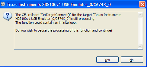
I have access to the DDR2 (read and write) from the JTAG emulator, after loading one of the GEL (both cases below), but sometimes the verification fails, and always (if any section in the linker file has been allocated to reside on the DDR2) the program loading fails.

The LogicPD GEL usually runs without hangs, but it seems that either the timers or/and the refresh rate values are incorrect. (Regardless if I use the spreadsheet values, or any other).

The second GEL, which includes sequence I wrote based on the TI DSP DDR2 documentation, halts (see below where), and beside doesn't improve the behavior of loading program which some of its sections are linked to reside on the DDR2.


Any idea?


Regards,

Uri


GEL based on the LogicPD example:

/**********************************************************************************
  mDDR Configuration routine:
    1. mDDR Enable
    2. VTP calibration
    3. Configure DDR
    4. Set to self-refresh, enable mclkstop and DDR Sync Reset
    5. Enable DDR and disable self-refresh

  int freq is MHz

***********************************************************************************/

DEVICE_mDDRConfig(unsigned int freq)
{
    int i;

    GEL_TextOut("\tDEVICE_mDDRConfig %d MHz","Output",1,1,1, freq);

    /*Enable the Clock to EMIF3A SDRAM*/
    PSC1_LPSC_enable(PD0, LPSC_DDR);

    // If VTP claiberation enabled , then skip the VTP calibration
    if((VTPIO_CTL & 0x00000040))
    {
       // Begin VTP Calibration
       VTPIO_CTL |= (0x00004000);     // Set IOPWRDN bit to enable input buffer powerdown enable mode
       VTPIO_CTL &= ~(0x00000040);  // Clear POWERDN bit (enable VTP)
      
       // Pulse (low) CLRZ to initiate VTP IO Calibration
       VTPIO_CTL |= (0x00002000);       // Set CLRZ bit
       VTPIO_CTL &= ~(0x00002000);    // Clear CLRZ bit (CLRZ should be low for at least 2ns)
       VTPIO_CTL |= 0x00002000;       // Set CLRZ bit

       // Polling READY bit to see when VTP calibration is done
       while(!((VTPIO_CTL & 0x00008000)>>15)) {}

       VTPIO_CTL |= 0x00000080;        // Set LOCK bit for static mode
       VTPIO_CTL |= 0x00000100;     // Set PWRSAVE bit to save power
       // End VTP Calibration
    }

    EMIF3A_SDCR |= 0x00800000; // Set BOOTUNLOCK

    // **********************************************************************************************
    // Setting based on 512Mb DDR MT47H32M16 on DSMP
    // Config DDR timings
    DDRCTL      = (0x0               << 8)   |  // Reserved
                  (0x1               << 7)   |  // EXT_STRBEN
                  (0x1               << 6)   |  // PWRDNEN
                  (0x0               << 3)   |  // Reserved
                  (0x4               << 0);     // RL

    EMIF3A_SDCR = (EMIF3A_SDCR & 0xF0000000) |  // Reserved
                  (0x0               << 27)  |  // DDR2TERM1
                  (0x1               << 26)  |  // IBANK_POS
                  (0x0               << 25)  |  // MSDRAMEN
                  (0x0               << 24)  |  // DDRDRIVE1
                  (0x0               << 23)  |  // BOOTUNLOCK
                  (0x0               << 22)  |  // DDR2DDQS
                  (0x0               << 21)  |  // DDR2TERM0
                  (0x1               << 20)  |  // DDR2EN
                  (0x0               << 19)  |  // DDRDLL_DIS
                  (0x0               << 18)  |  // DDRDRIVE0
                  (0x1               << 17)  |  // DDREN
                  (0x1               << 16)  |  // SDRAMEN
                  (0x1               << 15)  |  // TIMUNLOCK
                  (0x1               << 14)  |  // NM
                  (0x0               << 12)  |  // Reserved
                  (0x3               << 9)   |  // CL
                  (0x0               << 7)   |  // Reserved
                  (0x2               << 4)   |  // IBANK
                  (0x0               << 3)   |  // Reserved
                  (0x2               << 0);     // PAGESIZE

    // Subtracting 0.5 instead of 1 so that the int is rounded up after truncating a real value
    EMIF3A_SDTIMR1 = (((unsigned int) ((97.5 * freq / 1000) - 0.5)) << 25) |  // tRFC
                     (((unsigned int) ((18.0 * freq / 1000) - 0.5)) << 22) |  // tRP
                     (((unsigned int) ((18.0 * freq / 1000) - 0.5)) << 19) |  // tRCD
                     (((unsigned int) ((15.0 * freq / 1000) - 0.5)) << 16) |  // tWR
                     (((unsigned int) ((42.0 * freq / 1000) - 0.5)) << 11) |  // tRAS
                     (((unsigned int) ((60.0 * freq / 1000) - 0.5)) << 6)  |  // tRC
                     (((unsigned int) ((12.0 * freq / 1000) - 0.5)) << 3)  |  // tRRD
                     (EMIF3A_SDTIMR1 & 0x4)                                |  // Reserved
                     (((unsigned int) ((2.0 * freq / 1000) - 0.5))  << 0);    // tWTR

    // Subtracting 0.5 instead of 1 so that the int is rounded up after truncating a real value
    // tRASMAX is rounded down so subtracting 1
    // CAS/CL = 3
    EMIF3A_SDTIMR2 = (EMIF3A_SDTIMR2 & 0x80000000)                           |  // Reserved
                     (((unsigned int) ((70000 * freq / 1000) - 1))   << 27)  |  // tRASMAX
                     (0x0                                            << 25)  |  // tXP
                     (0x0                                            << 23)  |  // tODT (Not supported)
                     (((unsigned int) ((120.0 * freq / 1000) - 0.5)) << 16)  |  // tXSNR
                     ((200 - 1)                                      << 8)   |  // tXSRD (200 Cycles)
                     ((1 - 1)                                        << 5)   |  // tRTP (1 Cycle)
                     (0x0                                            << 0);     // tCKE
 

    EMIF3A_SDCR2   = 0x00000004; // 8K rows
 
    EMIF3A_SDRCR   = (0x1                                          << 31)  |  // LPMODEN
                     (0x1                                          << 30)  |  // MCLKSTOPEN
                     (0x0                                          << 24)  |  // Reserved
                     (0x0                                          << 23)  |  // SR_PD
                     (0x0                                          << 16)  |  // Reserved
                    /* (((unsigned int) ((7.8 * freq) + 0.5))         << 0);     // RR*/
                     (((unsigned int) ((3.9 * freq) + 0.5))        << 0);

    /*SyncReset the Clock to EMIF3A SDRAM*/
    PSC1_LPSC_SyncReset(PD0, LPSC_DDR);

    /*Enable the Clock to EMIF3A SDRAM*/
    PSC1_LPSC_enable(PD0, LPSC_DDR);

    EMIF3A_SDRCR &= ~0xC0000000;  // disable self-refresh
   
    EMIF3A_SDCR    &= ~0x00008000; // Clear TIMUNLOCK
}


GEL based on the TI documentation:

/*********************************************************************************
2.13.2 Initializing Following Device Power Up and Device RESET

    Following device power up, the DDR2/mDDR memory controller is held in reset with the internal clocks to
    the module gated off. Before releasing the DDR2/mDDR memory controller from reset, the clocks to the
    module must be turned on. Perform the following steps when turning the clocks on and initializing the
    module:
        1. Program PLLC1 registers to start 2X_CLK. For information on programming PLLC1, see your
        device-specific System Reference Guide.
        2. Program Power and Sleep Controller (PSC) to enable the DDR2/mDDR memory controller VCLK.
        3. Perform VTP IO calibration
            a. Clear CLKRZ, LOCK, and POWERDN bits in the VTP IO control register (VTPIO_CTL) and wait at
            least 1 reference clock cycle. You must wait at least 1 reference clock cycle for the CLKRZ to take
            affect. The reference clock is the clock at MXI/MXO.
            b. Set CLKRZ bit in VTPIO_CTL.
            c. Poll READY bit in VTPIO_CTL until it changes to logic-high.
            d. Set IOPWRDN bit in VTPIO_CTL.
            e. Set LOCK bit in VTPIO_CTL.
            f. Set POWERDN bit in VTPIO_CTL to save power. VTP is locked and no dynamic calibration will
            happen.
        4. Configure the DDR PHY control register 1 (DRPYC1R). All of the following steps may be done in a
        single register write to DRPYC1R.
            a. Set the EXT_STRBEN bit to 1 to select external DQS strobe gating.
            b. Program the RL bit to the required value.
        5. Program the Power and Sleep Controller (PSC) to reset (synchReset) the DDR2/mDDR memory
        controller.
        6. Configure the peripheral bus burst priority register (PBBPR). You must change its default value. See
        Section 4.8.
        7. Follow the register initialization procedure described in Section 2.13.1 to complete the DDR2/mDDR
        memory controller configuration.

2.13.1 Initializing Configuration Registers       
    Perform the following steps when configuring the DDR2/mDDR memory controller memory-mapped
    registers:
        1. Program the read latency (RL) bit in the DDR PHY control register (DRPYC1R) to the desired value.
        2. Program the SDRAM configuration register (SDCR) with BOOTUNLOCK bit set to 1 (unlocked).
        3. Program the SDRAM configuration register (SDCR) to the desired value with the BOOTUNLOCK
        cleared to 0 and the TIMUNLOCK bit set to 1 (unlocked).
        4. For mDDR only, program the SDRAM configuration register 2 (SDCR2) to the desired value.
        5. Program the SDRAM timing register 1 (SDTIMR1) and SDRAM timing register 2 (SDTIMR2) to the
        desired values to meet the DDR2/mDDR SDRAM memory data sheet specification.
        6. Program SDCR to the desired value with the TIMUNLOCK bit cleared to 0 (locked).
        7. Program the RR bit in the SDRAM refresh control register (SDRCR) to the desired value to meet the
        refresh requirements of the DDR2/mDDR SDRAM memory.
*********************************************************************************/

VTPIO_calibtarion() {
    // If VTP claiberation enabled , then skip the VTP calibration
    if((VTPIO_CTL & 0x00000040)) Taken from LogicPD example since TI sequence hangs
    {
       // Begin VTP Calibration
       VTPIO_CTL |= (0x00004000);     // Set IOPWRDN bit to enable input buffer powerdown enable mode
       VTPIO_CTL &= ~(0x00000040);  // Clear POWERDN bit (enable VTP)
      
       // Pulse (low) CLRZ to initiate VTP IO Calibration
       VTPIO_CTL |= (0x00002000);       // Set CLRZ bit
       VTPIO_CTL &= ~(0x00002000);    // Clear CLRZ bit (CLRZ should be low for at least 2ns)
       VTPIO_CTL |= 0x00002000;       // Set CLRZ bit

       // Polling READY bit to see when VTP calibration is done
       while(!((VTPIO_CTL & 0x00008000)>>15)) {}

       VTPIO_CTL |= 0x00000080;        // Set LOCK bit for static mode
       VTPIO_CTL |= 0x00000100;     // Set PWRSAVE bit to save power
       // End VTP Calibration
    }


      /* 2.13.2    [3] */
    // VTP IO calibration

    #define VTP_CLKRZ            (0x00002000)
    #define VTP_LOCK            (0x00000080)
    #define VTP_POWERDN            (0x00000040)
    #define VTP_READY            (0x00008000)
    #define VTP_READY            (0x00004000)
    //    VTPIO_CTL &= ~( VTP_CLKRZ | VTP_LOCK | VTP_POWERDN );    // a
    //    for (i = 0; i++; i<10) {}                                // a
    //    VTPIO_CTL |= VTP_CLKRZ;                                    // b
    //    while(!((VTPIO_CTL & VTP_READY) >> 15)) {}                // c Hangs here
    //    VTPIO_CTL |= VTP_READY;                                    // d
    //    VTPIO_CTL |= VTP_LOCK;                                    // e
    //    VTPIO_CTL |= VTP_POWERDN;                                // f
}


DEVICE_mDDRConfig(unsigned int freq) {
    int i;

   
    #define DRPYC1R                (DDRCTL)

    #define SDCR2_BOOTUNLOCK    (0x00800000)
    #define SDCR2_TIMUNLOCK        (0x00008000)

   
    GEL_TextOut("\tDEVICE_mDDRConfig %d MHz","Output",1,1,1, freq);
   
    /* 2.13.2    [1] */
    // Done @ device_PLL1()

    GEL_TextOut("\t2.13.2    [2]","Output",1,1,1);
    /* 2.13.2    [2] */
    // Enable the Clock to EMIF3A SDRAM/DDR
    PSC1_LPSC_enable(PD0, LPSC_DDR);

    GEL_TextOut("\t2.13.2    [3]","Output",1,1,1);
    /* 2.13.2    [3] */
    // VTP IO calibration
    VTPIO_calibtarion();
   
    GEL_TextOut("\t2.13.2    [4]","Output",1,1,1);
    /* 2.13.2    [4] */
    // DDR PHY control register 1
    DRPYC1R = 0x84; // EXT_STRBEN = External strobe. RL = (CAS latency + 1)
   
    GEL_TextOut("\t2.13.2    [5]","Output",1,1,1);
    /* 2.13.2    [5] */
    // PSC reset
//    PSC1_LPSC_SyncReset(PD0, LPSC_DDR);
Hangs here
//    PSC1_LPSC_enable(PD0, LPSC_DDR);   Hangs here

    GEL_TextOut("\t2.13.2    [6]","Output",1,1,1);
    /* 2.13.2    [6] */
    // 00h will ensure master priority is strictly honored (at the cost of decreased
    // DDR2/mDDR memory controller efficiency)
    EMIF3A_PBBPR = 0;
   
    GEL_TextOut("\t2.13.1    [2]","Output",1,1,1);
    /* 2.13.1    [2] */
    // Program the SDRAM configuration register (SDCR) with BOOTUNLOCK bit set to 1 (unlocked).
    EMIF3A_SDCR |= SDCR2_BOOTUNLOCK;
    EMIF3A_SDCR |= SDCR2_TIMUNLOCK;
   
    GEL_TextOut("\t2.13.1    [3]","Output",1,1,1);
    /* 2.13.1    [3] */
    EMIF3A_SDCR = 0x0013C622; // BOOTUNLOCK locked
   
    GEL_TextOut("\t2.13.1    [4]","Output",1,1,1);
    /* 2.13.1    [4] */
    // SDCR2
    EMIF3A_SDCR2   = 0x00000004; // 8K rows  

    GEL_TextOut("\t2.13.1    [5]","Output",1,1,1);
    /* 2.13.1    [5] */
    // Timers
    EMIF3A_SDTIMR1 = 0x1E922A09;
    EMIF3A_SDTIMR2 = 0x000000C4;
   
    GEL_TextOut("\t2.13.1    [6]","Output",1,1,1);
    /* 2.13.1    [6] */
    // TIMUNLOCK locked
    EMIF3A_SDCR &= ~(SDCR2_TIMUNLOCK);
   
    GEL_TextOut("\t2.13.1    [7]","Output",1,1,1);
    /* 2.13.1    [7] */
    // Refresh rate
    EMIF3A_SDRCR = 0x00000249;
}

  • Uri Shkolnik said:
    My environment is C6748 @ 300MHz, the DDR2 is 400MHz capable

    Is this your own board or do you have a LogicPD EVK? The GEL file that ships with the EVK should be the one that you start from and make sure it works at the speed it is designed for operating. Then use that same GEL file and get it working at the same speed on your own board, and then you should find a few places to change to get the different performance you are looking for.

    What hardware and software is known to be working in your system already?

  • My own custom board.


    I'm not so sure regarding "The GEL file that ships with the EVK should be the one that you start from".... it contradicts TI's documentation for multiple parameters.


    Uri

  • Uri

    Partial answer specifically for your PSC hang condition

    We recently found that the sequence in the DDR2 user guide is slightly incorrect. This is going to be fixed in the upcoming revision of the user guide ( regret the inconvenience).

    Uri Shkolnik said:
    5. Program the Power and Sleep Controller (PSC) to reset (synchReset) the DDR2/mDDR memory
            controller.
            6. Configure the peripheral bus burst priority register (PBBPR). You must change its default value. See
            Section 4.8.
            7. Follow the register initialization procedure described in Section 2.13.1 to complete the DDR2/mDDR
            memory controller configuration.

    Instead of 5-6-7, if you do 7-5-6 that should take care of the hangs in the PSC sections of the gel file you created. Note you will still need to write to SDRCR register the way it is done in the LogicPD gel file ( details below)

    ----

    More details: Essentially to allow the PSC to do a local Sync Reset, they key is to have the following bits in the SDRCR set to 1, as in the LogicPD gel file

    Uri Shkolnik said:

    EMIF3A_SDRCR   = (0x1                                          << 31)  |  // LPMODEN
                                          (0x1                                          << 30)  |  // MCLKSTOPEN

    Without this PSC will not be able to execute the syncreset on the EMIF controller.

    --

    Side NOTE: I see that you are setting PBBPR = 0h. I would strictly advise against that, as by doing so you are completely disabling the EMIF controllers ability to smartly optimize the commands that it gets from various masters in the system ( a 0x20 value instead of default 0xFF is recommended, unless more fine tuning is required)

    Some details on that here

  • Mukul,


    Regarding the SDRCR - After I Sync Reset the PSC, should I turn off these bits (LPMODEN and MCLKSTOPEN) or leave them set?


    Regards,

    Uri

  • Uri

    You can turn these bits off after the sequence.

    If you are not considering putting the DDR2/mDDR into low power modes or disabling the PLL1 clock source (MCLK) to the DDR2 controller for power savings, as highlighted in the user guide ( sections  2.8, 2.10, 2.16 in the user guide) , then these bits are not relevant. If you were to implement your own power management schemes for the external memory, then you could follow the steps highlighted in those sections (which includes settings those bits).

    Specifically, in the initialization sequence ,  these bits need to be set, because the DDR2 controller will disallow any  clock/reset transitions (those managed by PSC) if these bits are not set, and therefore your code hangs there doing the local reset (SyncReset on the DDR2 controller module).

    Regards

    Mukul

  • Seems that is works.... will test further in the next couple of days,


    Thanks,

    Uri

  • Hi Uri

    Good to see that the hang issue is resolved. Now back to your more critical issue on your Gel file not working and giving you loading errors, and the error messages below


    C674X_0: Output:     DDR init for 150 MHz is done
    C674X_0: Output:     ---------------------------------------------
    C674X_0: File Loader: Data verification failed at address 0xC0009400 Please verify target memory and memory map.
    Error found during data verification.
    Ensure the linker command file matches the memory map
    .


    I probably need to spend some time looking at your DDR2 register settings and make sure they are ok ( can you share your work spreadsheet that you used to calculate the values for your DDR2 memory).

    You mentioned that using the LogicPD GEL file your setup is more stable? Can you confirm that this is w.r.t to your custom board? Can you also elaborate on your original post  comments( I am not sure I get this, are you saying you don't get the above error with the LogicPD gel file on your custom board)

    >>The LogicPD GEL usually runs without hangs, but it seems that either the timers or/and the refresh rate values are incorrect. (Regardless if I use the spreadsheet values, or any other).

    Also, back to Randy's email/queries, are you confident that 150 MHz works on your custom board (trying to see if you have hardware or software issues). Can you also try running at a lower frequency (132 or 125MHz)?

    Regards

    Mukul

  • Mukul,

    Eric Wilbur here. I have been using the C6748 EK for a few months now and consistently get "OnTargetConnect() not running atomically" error during connection to the target. I.e. it hangs. If you continue loading your code, the green Play button is greyed out because the GEL is stuck in an infinite loop in the mDDR init section. If I terminate debug, then relaunch the debugger, most of the time the program loads. This problem is consistent enough to be more than an instability - more like a bug.

    I'm using the latest 6748 GEL file from LogicPD. Has anyone else experienced a problem like this? Has anyone created a "stable' C6748.gel file?

    Below is the "message". Also, when I load code after the GEL file runs correctly, I often get stuck at _c_int00 and the debugger is "running" already - never gets to main(). I'm not sure if the problems are related.

    Thanks,

    Eric

  • Mukul,

    I am looking at my gel file (actually LogicPD's) and doing a side-by-side comparison with your 5-6-7 vs. 7-5-6 statement. I'm lost. Is it possible for you to post a modified C6748 GEL file that I can use temporarily while I'm developing some code for the BIOS workshop? Whatever changes you think are necessary, I think the community out here would all appreciate a more stable gel file for the C6748 EVM. Even if you just make the changes to the GEL file that you mentioned above.

    Or, I'd be happy to receive an email.

    Thanks...cause I'm stuck with that beautiful message starting at me above without it...

    ;)


  • Eric

    I believe the LogicPD Gel files do not have any issue. On this thread, Uri was trying to create a gel file sequence based on our mDDR/DDR2 userguide sequence (Section 2.13.2) which is currently incorrect.

    The sequence in the Logic PD GEL is fine, I am showing the partially truncated sequence from the logicPD c6748 gel file below

    --------


    DEVICE_mDDRConfig(unsigned int freq)
    {
        /*Enable the Clock to EMIF3A SDRAM*/
        PSC1_LPSC_enable(PD0, LPSC_DDR);

       :

       :

       :

       (snip )

        EMIF3A_SDCR2   = 0x00000000; // IBANK_POS set to 0 so this register does not apply
        EMIF3A_SDRCR   = (0x1                      << 31)  |  // LPMODEN
                         (0x1                                          << 30)  |  // MCLKSTOPEN

                         (0x0                                          << 24)  |  // Reserved
                         (0x0                                          << 23)  |  // SR_PD
                         (0x0                                          << 16)  |  // Reserved
                         (((unsigned int) ((7.8125 * freq) + 0.5))     << 0);     // RR

    /*SyncReset the Clock to EMIF3A SDRAM*/
        PSC1_LPSC_SyncReset(PD0, LPSC_DDR);

        /*Enable the Clock to EMIF3A SDRAM*/
        PSC1_LPSC_enable(PD0, LPSC_DDR);


        EMIF3A_SDRCR &= ~0xC0000000;  // disable self-refresh
    }

    -------

    The key is to have the lines highlighted in red done before (as part of the Step 7 in Section 2.13.2) BEFORE you do the LPSC SyncReset and LPSC Enable calls.

    You might find Brad Griffis post on OMAPL138 also useful

    http://e2e.ti.com/support/dsp/omap_applications_processors/f/42/p/51874/183863.aspx#183863

    If you have any additional questions/confusions let me know.

    Regards

    Mukul

  • I have the same problem as Eric [ed: referenced thread DDR2 Initialization (GEL)]. Whenever I try to run the debugger a second time (after a hard reset) it will hang and finally the debugger will abort with an error message.

    I am using the LogicPD Zoom eXperimenter Kit with AM1808 controller. Debugging is done with CCS 4.1.1 and Blackhawk USB100v2. The GEL file (AM1808.gel, v 1.0, 2/25/2010) from LogicPD is used. The GEL-file differs in one line from Uri's:

    ==================================

    DEVICE_mDDRConfig(unsigned int freq)


    {

    /*Enable the Clock to EMIF3A SDRAM*/

    PSC1_LPSC_enable(PD0, LPSC_DDR);

    /*If VTP claiberation enabled , then skip the VTP calibration*/

    if((VTPIO_CTL & 0x00000040))

    {

    // Begin VTP Calibration

    VTPIO_CTL |= (0x00004000); // Set IOPWRDN bit to enable input buffer powerdown enable mode

    VTPIO_CTL &= ~(0x00000040); // Clear POWERDN bit (enable VTP)

    // Pulse (low) CLRZ to initiate VTP IO Calibration

    VTPIO_CTL |= (0x00002000); // Set CLRZ bit

    VTPIO_CTL &= ~(0x00002000); // Clear CLRZ bit (CLRZ should be low for at least 2ns)

    VTPIO_CTL |= 0x00002000; // Set CLRZ bit

    // Polling READY bit to see when VTP calibration is done

    while(!((VTPIO_CTL & 0x00008000)>>15)) {}

    VTPIO_CTL |= 0x00000080; // Set LOCK bit for static mode

    VTPIO_CTL |= 0x00000100; // Set PWRSAVE bit to save power

    VTPIO_CTL |= 0x00000040; // Set POWERDN bit to power down VTP module

    // End VTP Calibration

    }

    EMIF3A_SDCR |= 0x00800000; // Set BOOTUNLOCK

    ...

    ==================================

    ....

    In contrast to Uri's version the VTP module is powered down after calibration. If this line is removed, the second debug run will work (probably because "VTPIO_CTL & 0x00000040" evaluates to false and hence the while-loop is not entered).

    Is it necessary to disable the VTP module after calibration? If yes, is there another way to solve this problem? Maybe by triggering a reset of the CPU via the GEL file.

    Thanks in advance.


  • If the highlighted line is removed from the GEL and your debugging works better, then please comment out that line.

    Is your GEL file older or newer than the one Uri was using? You might want to go back to the LogicPD site to see if they have an update to these support files. You may also want to update your CCS installation to the latest version.

    According to the documentation, there is no good reason to set both PWRSAVE and POWERDN. Setting PWRSAVE has no effect if POWERDN is set. So it makes sense to leave off the POWERDN line, especially since it works that way.

    Regards,
    RandyP