This thread has been locked.

If you have a related question, please click the "Ask a related question" button in the top right corner. The newly created question will be automatically linked to this question.

raw capture on dm6437

Hi!

I am making a software using video_loopback as basis with the sensor MT9P031 (using XGA (2048x1536) configuration).
Following the user´ s guide SPRU977 – VPFE (figure 11 up to 17) I had set the follow registers:
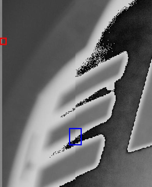
VPSS_CLKCTL.PLKINV = 0 // VENC clock mux and CCD receive noninverted PCLK
SYS.MODE.DATAPOL = 0 // normal
SYS_MODE.DATSIZ = 4 // 12 bits
DCSUB.DCSUB = 0 // DC level to subtract from CCD data
CLAMP.CLAMPEN = // disable
SYN_MODE.INPMOD = 0 // CCD raw data
COLPTN = 0xBB11BB11
BLKCMP = 0
FCP.FPCEN = 0 // disable
FMTCFG.VPEN = 0 // disable
SYN_MODE.VP2SDR = 0
HORZ_INFO.SPH = 0
HORZ_INFO.NPH= 0x7FF
VERT_START.SLV0 = 0
VERT_START.SLV1 = 0
VERT_LINES.NLV = 0x5FF
SYN_MODE.LPF = 0
ALAW.CCDTBL = 0
HSIZE_OFF.LNOFST = 0x00001000
SDOFST = 0x00000249
SYN_MODE.WEN = 1 //enable

After it, the image never comes into DDR and the CCDC is never busy.
Someone have an idea what I’ m doing wrong?
Thanks!

  • I configured the PINMUX0 and it (PCR) busy now!!

    Now, I dont know how can I read the data on memory......
    Someone know can I do it??

    Thanks!


  • My sensor give me RGB image data (12bits), and it is stored into DDR
      G      R    B    R
    0000 XXXX XXXX XXXX  0000 XXXX XXXX XXXX  0000 XXXX XXXX XXXX  0000 XXXX XXXX XXXX 

    When I use A-law table
             G              R     B          R
    XXXX XXXX   XXXX XXXX    XXXX XXXX   XXXX XXXX 

    Am I wrong?


    Thanks

  • It looks proper.

    FYI, A-law is lossy compression to store Raw data in 8bit (1byte). If you use A-law, then Inverse A-law should be used for processing.


    regards,

    Sang-Yong


  • Hi Sang-Yong!

    Ok, but how can I to configure the Graphic Property Dialog to see the image into DDR?

    I configured like this:

    Color Space - RGB

    Interleaved Data Source - No

    Start Address – R Source – buffer

    Start Address – G Source – buffer

    Start Address – B Source – buffer

    Line per Display – 720

    Pixel per Line – 1024

    Byte Packing to fill 32 bits – No

    Index Increments – 2

    Image Origin – Top Left

    Uniform Quantization to 256 Colors – No


    And the image appear different of real.


    Thankyou. 

  •  

    Now I can see the image in the graphic view! But some think is happening…

    Follow just a little part of image. The entire image is 1024x720. 

    In the red part, the 4 first columns is like the (around of) columns 160 of the image.

    I don’t know if because this happen the break of image in the blue part.

    Do you know why this is happen, and how can I fix it?

    Thanks

  • I don't use Graphic view, so I don't have good idea.

    But the image looks compressed. Did you compress the data for posting?

    Also, I see first 7columns are different and (I believe) it isn't related to the gap in column 160.

    I think this is Raw data, right?

    Did you take out blank data properly? So you write the image area only to memory?

    I don't have any clue about the gap in column 160, but is this the only gap you see in 1024 columns?


    Regards,

    Sang-Yong


  • Yes, I compressed the image and I just put a part of image.

    And there are first 4 columns different.

    It is a raw data, and I just write into ddr.

    I did some tests here setting the sensor with different resolutions, and I saw that first 4 columns copy different positions…. For example, in the VGA resolution, they copy around of column 160, in the XGA resolution they copy around of column 900….. it is very strange….

    That part of image than is break (or gap), in the all resolution break in the same potion. (Between 123 to 124 column).

    Some idea?


    Thanks


  • Could you save the data and share it?


    Regards,

    Sang-Yong

  • Sure

    !

    This image is VGA (640x480). 

    In this image, the first 4 columns are equal, around of, column 255, and the gap appear between column 123 and 124.

    Thanks


  • I am sorry for unclear request, but I asked Raw data itself, instead of viewer output.

    Also it might be helpful, if you capture recognizable scene.

    By the way, the column number of gap is always same if you fix image size?


    Regards,

    Sang-Yong 

  • The raw data do you mean the data than I read of sensor and write into ddr? How can I share the raw data?? 

     And yes, the column number of gap always the same independent the sensor configuration (size and resolution).


    Thanks

  • If you are OK to post the Raw data, then please use File Attachment in "Options" tab.


    regards,

    Sang-Yong

  • Sorry, but I didn’t understand what do you means about share raw data… is it the image than I post here?

    Please, give me step by step what I need to do… principally if I need to do (or get) some think in the CCS….


    Thanks


  • Marcio,

    Just to add, you can do a "Memory Save" option in CCS to save the R, G, B data buffers to local files on your PC. This way you can dump the complete data and share with us so that we can analyze it. Please ensure that you save the data in binary format and not in "hex" format.

    Regards,

    Anshuman

  • Hi Anshuman

    How can I save the data in binary format? 

    To save data I selected File -> Data -> Save

    And there are not the option to save data in the binary format, there are hex, integer, long, float, addressable unit, coff and all files.

    Am I doing some think wrong?


    Thanks


  • Hi!

    Someone knows how can I save data image in binary format from CCS?

    Thanks!


  • Marcio,

    Which version of CCS are you using? If you are using CCS 3.3 onwards, you should be able to see Tools->Memory Save/Load Utility. This should help you to save the data from CCS.

    Regards,

    anshuman

  • Hi Anshuman

    I am using CCS 3.3, but there is not this option (Memory Save/ Load Utility) in the Tools..... There are Data Converter Support, Simulator Analysis, Command Window, Port Connect, Pin Connect, OS Selector, Kernel/ Object View, RTDX, Cache Viewer Control, XDS560 Trace and Advanced Event Triggering.

    Some Idea?

    Thanks!


  • Hi

    Another question, why I capture the full frame when I configure the CCDC_PCR = 0 in the time less of the 1 frame?

    Let me explain better:

    CCDC_PCR = 1; // enable capture
    while (CCDC_PCR == 1) { // waiting for busy
    }
    while (CCDC_PCR == 3) { // while busy
    }
    CCDC_PCR = 0; // disable capture

    This is have sense to capture 1 frame, but...

    CCDC_PCR = 1; // enable capture
    _waitus(500); // time less than 1 frame
    CCDC_PCR = 0; // disable capture

    In this form I captured 1 frame also! Why it is happen??

    Thanks


  • Below is a copy from DM644x VPFE doc. DM643x has the same ISP, so this can be applied as it is. As shown below, Enable bit is Shadowed register, so it is applied when new frame starts.

    Hope you can have time to check the document.

    Regards,

    Sang-Yong


     http://www.ti.com/litv/pdf/sprue38f

    5.4.4 Register Accessibility During Frame Processing
    There are three types of register access in the CCD controller:
    • Shadowed registers. In the CCD controller, there are three different register fields that are shadowed
    in different ways. Shadowed registers are those that can be read and written at any time, but the
    written values only take effect (are latched) at certain times based on some event. Note that reads will
    still return the most recent write even though the settings are not used until the specific event occurs.
    The following register/fields are shadowed:
    – PCR.ENABLE: Written values take effect only at the start of a frame event (rising edge of VD, if
    SYN_MODE.VDPOL is positive; falling edge of VD, if SYN_MODE.VDPOL is negative).
    – SDR_ADDR: When CCDCFG.VDLC is cleared to 0, written values take effect only at the start of a
    frame event (rising edge of VD, if SYN_MODE.VDPOL is positive; falling edge of VD, if
    SYN_MODE.VDPOL is negative). When CCDCFG.VDLC is set to 1, written values take effect only
    at the start of the frame being output to SDRAM (when the input has reached the
    HORZ_INFO.SPH pixel of the VERT_START.SLVn line of each field).
    – CCDCFG.YCINSWP: Written values take effect only during the active period of VD (when VD is
    high, if SYN_MODE.VDPOL is positive; when VD is low, if SYN_MODE.VDPOL is negative).

  • Thak you Sang-Yong!

    Now it has sense!

    Do you know how can I get the binary image (at CCS) for I share the image with you? I cant to resolve that problem (the gap problem) yet.....

    Thaks!


  • Hi!

    Someone know how can I save binary image (at CCS Vs3.3) for I attach here?

    Thanks!


  • Hi everybody!

    Finally I found the raw image problem!!!!!!!!!

    I created a buffer (in this case Uint16 ImageData[500000]) to save the raw image from VPFE. 

    The program created this buffer at position 0x80010008 into the memory, and because of this position, my image come with that gap!

    To resolve this problem I created this buffer using #pragma DATA_ALING(ImageData,32), and the program created at 0x80010020.


    Why the position of the buffer interfere in the image?


    Thanks!


  • Great to hear that you solve the issue. Hope we can support better, but please read our TRM carefully as it shows many detail information.

    One potential issue I can see is the address alignment. I copied a part of information related to the addres.

    Regards,

    Sang-Yong


    6.1.12 SDR_ADDR - SDRAM Address
    SDR_ADDR offset: 44
    CCDC - SDR_ADDR 0x01C7:042C
    Bit 31- 0
    Name SDR_ADDR
    R/W R/W
    Default 0
    Bit Field Description
    31-0 SDR_ADDR
    32-bit SDRAM starting address for CCDC output
    *This bit field is latched by VD
    Note that the address should be aligned on a 32_byte boundary. Therefore, the 5 LSB's are
    ignored. Furthermore, reading this register will always show the 5 LSB's as 0.
    For optimal performance in the system, the address should be on a 256-byte boundary.


  • http://e2e.ti.com/support/dsp/davinci_digital_media_processors/f/99/p/7311/350642.aspx#350642

    would you help me solve this problem? Is some ccdc reg setting  wrong?

    void vpfe_init( Uint32 buffer, Uint32 width, Uint32 height )
    {
     VPBE_VENC_VMOD      = 0x00000000u;
        VPBE_PCR            = 0x00000000u;
     VPSS_CLK_CTRL       = 0x00000018u;

        VPFE_CCDC_SYN_MODE  = 0
                            |(0<<19)      
                            |(0<<18)       
                            |(1<<17)      
                            |(1<<16)       
                            |(0<<15)       
                            |(0<<14)      
                            |(0<<12)      
                            |(0<<11)      
                            |(0<<8)        
                                           
                            |(0<<7)     
                            |(0<<6)       
                            |(0<<5)        
                                          
                            |(0<<4)       
                            |(1<<3)        
                            |(1<<2)        
                            |(0<<1)        
                            |(0);         

        VPFE_CCDC_HD_VD_WID = 0;           
        VPFE_CCDC_PIX_LINES = 0;  
                           
        VPFE_CCDC_HORZ_INFO = width << 1;
                                           
        VPFE_CCDC_HSIZE_OFF = width << 1;
                                                                             
        VPFE_CCDC_VERT_START = 0;         
                                                                
        VPFE_CCDC_VERT_LINES = height>>1;                          
        VPFE_CCDC_CULLING   = 0xFFFF00FF;                              
        VPFE_CCDC_SDOFST    = 0
                          |(0<<14)    
                          |(0<<12)     
                          |(0<<9)                 
                          |(0<<6)      
                          |(0<<3)                            
                          |(0<<0);                                   
        VPFE_CCDC_SDR_ADDR  = buffer; 
        VPFE_CCDC_CLAMP     = 0      
                          |(0<<31)        
                          |(0<<28)         
                          |(0<<25)        
                          |(0<<10)         
                          |(0<<0);          
        VPFE_CCDC_DCSUB     = 0;           
        VPFE_CCDC_COLPTN    = 0xEE44EE44;  
                     
        VPFE_CCDC_BLKCMP    = 0;          
                    
        VPFE_CCDC_FPC_ADDR  = 0x86800000;  
        VPFE_CCDC_FPC       = 0;
        VPFE_CCDC_VDINT     = 0;           
        VPFE_CCDC_ALAW      = 0;           
        VPFE_CCDC_REC656IF  = 0
                          |(0<<1)          
                          |(0<<0) ;         

        VPFE_CCDC_CCDCFG    = 0
                          |(0<<15)    
                          |(0<<13)    
                          |(0<<12)     
                                       
                          |(1<<11)   
                          |(0<<8)      
                          |(0<<6)     
                          |(0<<5)     
                          |(0<<4)      
                          |0;

        VPFE_CCDC_FMTCFG    = 0;
        VPFE_CCDC_FMT_HORZ  = 0
                          |(0x56<16)    
                          |(0x168<<0)     
                          |0;
        VPFE_CCDC_FMT_VERT  = 0
                          |(0xd<<16)     
                          |(0x64<<0)     
                          |0;
        VPFE_CCDC_FMT_ADDR0 = 0;
        VPFE_CCDC_FMT_ADDR1 = 0;
        VPFE_CCDC_FMT_ADDR2 = 0;
        VPFE_CCDC_FMT_ADDR3 = 0;
        VPFE_CCDC_FMT_ADDR4 = 0;
        VPFE_CCDC_FMT_ADDR5 = 0;
        VPFE_CCDC_FMT_ADDR6 = 0;
        VPFE_CCDC_FMT_ADDR7 = 0;
        VPFE_CCDC_PRGEVEN_0 = 0;
        VPFE_CCDC_PRGEVEN_1 = 0;
        VPFE_CCDC_PRGODD_0  = 0;
        VPFE_CCDC_PRGODD_1  = 0;
        VPFE_CCDC_VP_OUT    = 0  
                        |(0x63<<17)      
                        |(0x168<<4)       
                        |(0<<0);      
        VPFE_CCDC_PCR       = 0x00000001;  
       
    }