This thread has been locked.

If you have a related question, please click the "Ask a related question" button in the top right corner. The newly created question will be automatically linked to this question.

AM437x I2C1 sends only one byte

Other Parts Discussed in Thread: PCA9546A, AM4377

Dear All,

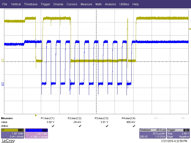
My team found that the use of AB18/AE18 for I2C1 (select from Pin Mux Tool) could only generate the 1st byte (slave address) with ACK (Low) from Device, no further clock and data for conmunication.

When we reworked to use G20/E25 for I2C1, the same configuration (OS,Driver,etc) resulted the I2C device read/write passed.

My team want to know whether AB18/AE18 could be configured as normal I2C Bus (I2C1) or any special cofiguration is required.

Arc Chen

I2C1 (SCL/AB18, SDA/AE18) waveform with only 1st byte:

  • Hi,

    There are no restrictions for pins AB18/AE18. Check that your pinmux settings do not get accidentaly overwritten on these pins by another driver.
  • Hi Biser,

    Here is the run-time status for AB18/AE18 register:
         root@am437x-evm:/# devmem2 0x44e10a08
         /dev/mem opened.
         Memory mapped at address 0xb6fba000.
         Read at address 0x44E10A08 (0xb6fbaa08): 0x00050003 <= AE18
         root@am437x-evm:/# devmem2 0x44e10a0c
         /dev/mem opened.
         Memory mapped at address 0xb6f3a000.
         Read at address 0x44E10A0C (0xb6f3aa0c): 0x00050003 <= AB18
    Accrounding to TRM, last 4-bits should be pin function select.
    Mode 3 of AB18/AE18 should be I2C1 SCL/SDA, I think overwritten should not happen right here.

    Best Regards,
    Wayne Kuo

  • Is this a custom board or the AM437x GP EVM?
  • Hi Biser,

    This result is on customer's board.
    They use 3 I2C buses for application, I2C0 and I2C2 is working fine.
    During the debuging, they find out the issue on AB18/AE18.

    Is there any other thing we can check next?
    Attachment is customer's device tree setting.

    Thank you and Regards,
    Wayne Kuo

    /*
     * Copyright (C) 2014 Texas Instruments Incorporated - http://www.ti.com/
     *
     * This program is free software; you can redistribute it and/or modify
     * it under the terms of the GNU General Public License version 2 as
     * published by the Free Software Foundation.
     */
    
    /dts-v1/;
    
    #include "am4372.dtsi"
    #include <dt-bindings/pinctrl/am43xx.h>
    #include <dt-bindings/pwm/pwm.h>
    #include <dt-bindings/gpio/gpio.h>
    #include <dt-bindings/input/input.h>
    
    / {
    	model = "TI AM437x Industrial Development Kit";
    	compatible = "ti,am437x-idk-evm","ti,am4372","ti,am43";
    
    	v24_0d: fixed-regulator-v24_0d {
    		compatible = "regulator-fixed";
    		regulator-name = "V24_0D";
    		regulator-min-microvolt = <24000000>;
    		regulator-max-microvolt = <24000000>;
    		regulator-always-on;
    		regulator-boot-on;
    	};
    
    	v3_3d: fixed-regulator-v3_3d {
    		compatible = "regulator-fixed";
    		regulator-name = "V3_3D";
    		regulator-min-microvolt = <3300000>;
    		regulator-max-microvolt = <3300000>;
    		regulator-always-on;
    		regulator-boot-on;
    		vin-supply = <&v24_0d>;
    	};
    
    	vdd_corereg: fixed-regulator-vdd_corereg {
    		compatible = "regulator-fixed";
    		regulator-name = "VDD_COREREG";
    		regulator-min-microvolt = <1100000>;
    		regulator-max-microvolt = <1100000>;
    		regulator-always-on;
    		regulator-boot-on;
    		vin-supply = <&v24_0d>;
    	};
    
    	vdd_core: fixed-regulator-vdd_core {
    		compatible = "regulator-fixed";
    		regulator-name = "VDD_CORE";
    		regulator-min-microvolt = <1100000>;
    		regulator-max-microvolt = <1100000>;
    		regulator-always-on;
    		regulator-boot-on;
    		vin-supply = <&vdd_corereg>;
    	};
    
    	v1_8dreg: fixed-regulator-v1_8dreg{
    		compatible = "regulator-fixed";
    		regulator-name = "V1_8DREG";
    		regulator-min-microvolt = <1800000>;
    		regulator-max-microvolt = <1800000>;
    		regulator-always-on;
    		regulator-boot-on;
    		vin-supply = <&v24_0d>;
    	};
    
    	v1_8d: fixed-regulator-v1_8d{
    		compatible = "regulator-fixed";
    		regulator-name = "V1_8D";
    		regulator-min-microvolt = <1800000>;
    		regulator-max-microvolt = <1800000>;
    		regulator-always-on;
    		regulator-boot-on;
    		vin-supply = <&v1_8dreg>;
    	};
    
    	v1_5dreg: fixed-regulator-v1_5dreg{
    		compatible = "regulator-fixed";
    		regulator-name = "V1_5DREG";
    		regulator-min-microvolt = <1500000>;
    		regulator-max-microvolt = <1500000>;
    		regulator-always-on;
    		regulator-boot-on;
    		vin-supply = <&v24_0d>;
    	};
    
    	v1_5d: fixed-regulator-v1_5d{
    		compatible = "regulator-fixed";
    		regulator-name = "V1_5D";
    		regulator-min-microvolt = <1500000>;
    		regulator-max-microvolt = <1500000>;
    		regulator-always-on;
    		regulator-boot-on;
    		vin-supply = <&v1_5dreg>;
    	};
    /*
    	gpio_keys: gpio_keys {
    		compatible = "gpio-keys";
    		pinctrl-names = "default";
    		pinctrl-0 = <&gpio_keys_pins_default>;
    		#address-cells = <1>;
    		#size-cells = <0>;
    
    		switch@0 {
    			label = "power-button";
    			linux,code = <KEY_POWER>;
    			gpios = <&gpio4 2 GPIO_ACTIVE_LOW>;
    		};
    	};*/
    };
    
    &am43xx_pinmux {
    	my_spi_0_pins_default: my_spi_0_pins_default {
    		pinctrl-single,pins = <
    			0x150 ( PIN_OUTPUT | MUX_MODE0 ) /* (P23) spi0_sclk.spi0_sclk */
    			0x154 ( PIN_INPUT | MUX_MODE0 ) /* (T22) spi0_d0.spi0_d0 */
    			0x158 ( PIN_OUTPUT | MUX_MODE0 ) /* (T21) spi0_d1.spi0_d1 */
    			0x15c ( PIN_OUTPUT_PULLUP | MUX_MODE0 ) /* (T20) spi0_cs0.spi0_cs0 */
    			0x274 ( PIN_OUTPUT_PULLUP | MUX_MODE1 ) /* (C24) xdma_event_intr1.spi0_cs2 */
    		>;
    	};
    	
    	/* Optional sleep pin settings. Must manually enter values in the below skeleton. */
    	
    	my_spi_1_pins_default: my_spi_1_pins_default {
    		pinctrl-single,pins = <
    			0x108 ( PIN_OUTPUT | MUX_MODE2 ) /* (D16) mii1_col.spi1_sclk */
    			0x10c ( PIN_INPUT | MUX_MODE2 ) /* (B14) mii1_crs.spi1_d0 */
    			0x110 ( PIN_OUTPUT | MUX_MODE2 ) /* (B13) mii1_rx_er.spi1_d1 */
    			0x144 ( PIN_OUTPUT_PULLUP | MUX_MODE2 ) /* (A16) rmii1_ref_clk.spi1_cs0 */
    			0x164 ( PIN_OUTPUT_PULLUP | MUX_MODE2 ) /* (G24) eCAP0_in_PWM0_out.spi1_cs1 */
    		>;
    	};
    	
    	/* Optional sleep pin settings. Must manually enter values in the below skeleton. */
    	
    	my_spi_2_pins_default: my_spi_2_pins_default {
    		pinctrl-single,pins = <
    			0x1b8 ( PIN_OUTPUT | MUX_MODE4 ) /* (AC18) cam0_field.spi2_sclk */
    			0x1bc ( PIN_INPUT | MUX_MODE4 ) /* (AD17) cam0_wen.spi2_d0 */
    			0x1b4 ( PIN_OUTPUT | MUX_MODE4 ) /* (AD18) cam0_vd.spi2_d1 */
    			0x1c0 ( PIN_OUTPUT_PULLUP | MUX_MODE4 ) /* (AC20) cam0_pclk.spi2_cs0 */
    			0x1b0 ( PIN_OUTPUT_PULLUP | MUX_MODE4 ) /* (AE17) cam0_hd.spi2_cs1 */
    		>;
    	};
    	
    	/* Optional sleep pin settings. Must manually enter values in the below skeleton. */
    	
    	my_spi_3_pins_default: my_spi_3_pins_default {
    		pinctrl-single,pins = <
    			0xd0 ( PIN_OUTPUT | MUX_MODE8 ) /* (C19) dss_data12.spi3_sclk */
    			0xd4 ( PIN_INPUT | MUX_MODE8 ) /* (D19) dss_data13.spi3_d0 */
    			0xd8 ( PIN_OUTPUT | MUX_MODE8 ) /* (C17) dss_data14.spi3_d1 */
    			0xdc ( PIN_OUTPUT_PULLUP | MUX_MODE8 ) /* (D17) dss_data15.spi3_cs0 */
    			0xcc ( PIN_OUTPUT_PULLUP | MUX_MODE8 ) /* (B18) dss_data11.spi3_cs1 */
    		>;
    	};
    	
    	/* Optional sleep pin settings. Must manually enter values in the below skeleton. */	
    	my_spi_4_pins_default: my_spi_4_pins_default {
    		pinctrl-single,pins = <
    			0x250 ( PIN_OUTPUT | MUX_MODE0 ) /* (P25) spi4_sclk.spi4_sclk */
    			0x254 ( PIN_INPUT | MUX_MODE0 ) /* (R24) spi4_d0.spi4_d0 */
    			0x258 ( PIN_OUTPUT | MUX_MODE0 ) /* (P24) spi4_d1.spi4_d1 */
    			0x25c ( PIN_OUTPUT_PULLUP | MUX_MODE0 ) /* (N25) spi4_cs0.spi4_cs0 */
    			0x230 ( PIN_OUTPUT_PULLUP | MUX_MODE2 ) /* (H22) uart3_ctsn.spi4_cs1 */
    		>;
    	};
    	
    	/* Optional sleep pin settings. Must manually enter values in the below skeleton. */
    
    	
    	my_gpio_0_pins_default: my_gpio_0_pins_default {
    		pinctrl-single,pins = <
    			0x1a8 ( PIN_OUTPUT | MUX_MODE9 ) /* (M25) mcasp0_axr1.gpio0[2] */
    			0x1ac ( PIN_OUTPUT | MUX_MODE9 ) /* (L24) mcasp0_ahclkx.gpio0[3] */
    			0x178 ( PIN_OUTPUT | MUX_MODE7 ) /* (K22) uart1_ctsn.gpio0[12] */
    			0x17c ( PIN_INPUT | MUX_MODE7 ) /* (L22) uart1_rtsn.gpio0[13] */
    			0x1a0 ( PIN_INPUT | MUX_MODE9 ) /* (L23) mcasp0_aclkr.gpio0[18] */
    			0x270 ( PIN_OUTPUT | MUX_MODE7 ) /* (D24) xdma_event_intr0.gpio0[19] */
    			0x268 ( PIN_INPUT | MUX_MODE9 ) /* (P20) spi2_d1.gpio0[21] */
    			0x260 ( PIN_OUTPUT | MUX_MODE9 ) /* (N20) spi2_sclk.gpio0[22] */
    			0x26c ( PIN_OUTPUT | MUX_MODE9 ) /* (T23) spi2_cs0.gpio0[23] */
    			0x278 ( PIN_INPUT | MUX_MODE7 ) /* (H20) clkreq.gpio0[24] */
    			0x28 ( PIN_INPUT | MUX_MODE7 ) /* (F11) gpmc_ad10.gpio0[26] */
    			0x70 ( PIN_INPUT | MUX_MODE7 ) /* (A2) gpmc_wait0.gpio0[30] */
    		>;
    	};
    	
    	/* Optional sleep pin settings. Must manually enter values in the below skeleton. */
    
    	
    	my_gpio_1_pins_default: my_gpio_1_pins_default {
    		pinctrl-single,pins = <
    			0x0 ( PIN_OUTPUT | MUX_MODE7 ) /* (B5) gpmc_ad0.gpio1[0] */
    			0x4 ( PIN_OUTPUT | MUX_MODE7 ) /* (A5) gpmc_ad1.gpio1[1] */
    			0x8 ( PIN_INPUT | MUX_MODE7 ) /* (B6) gpmc_ad2.gpio1[2] */
    			0xc ( PIN_OUTPUT | MUX_MODE7 ) /* (A6) gpmc_ad3.gpio1[3] */
    			0x10 ( PIN_OUTPUT | MUX_MODE7 ) /* (B7) gpmc_ad4.gpio1[4] */
    			0x14 ( PIN_OUTPUT | MUX_MODE7 ) /* (A7) gpmc_ad5.gpio1[5] */
    			0x18 ( PIN_OUTPUT | MUX_MODE7 ) /* (C8) gpmc_ad6.gpio1[6] */
    			0x1c ( PIN_INPUT | MUX_MODE7 ) /* (B8) gpmc_ad7.gpio1[7] */
    			0x30 ( PIN_OUTPUT | MUX_MODE7 ) /* (E11) gpmc_ad12.gpio1[12] */
    			0x34 ( PIN_INPUT | MUX_MODE7 ) /* (C11) gpmc_ad13.gpio1[13] */
    			0x38 ( PIN_OUTPUT | MUX_MODE7 ) /* (B11) gpmc_ad14.gpio1[14] */
    			0x3c ( PIN_INPUT | MUX_MODE7 ) /* (A11) gpmc_ad15.gpio1[15] */
    			0x78 ( PIN_INPUT | MUX_MODE7 ) /* (A3) gpmc_be1n.gpio1[28] */
    			0x80 ( PIN_INPUT | MUX_MODE7 ) /* (B9) gpmc_csn1.gpio1[30] */
    			0x84 ( PIN_OUTPUT | MUX_MODE7 ) /* (F10) gpmc_csn2.gpio1[31] */
    		>;
    	};
    	
    	/* Optional sleep pin settings. Must manually enter values in the below skeleton. */
    
    	
    	my_gpio_2_pins_default: my_gpio_2_pins_default {
    		pinctrl-single,pins = <
    			0xa4 ( PIN_OUTPUT | MUX_MODE7 ) /* (A21) dss_data1.gpio2[7] */
    			0xa8 ( PIN_OUTPUT | MUX_MODE7 ) /* (B21) dss_data2.gpio2[8] */
    			0xac ( PIN_OUTPUT | MUX_MODE7 ) /* (C21) dss_data3.gpio2[9] */
    			0xb0 ( PIN_OUTPUT | MUX_MODE7 ) /* (A20) dss_data4.gpio2[10] */
    			0xb4 ( PIN_OUTPUT | MUX_MODE7 ) /* (B20) dss_data5.gpio2[11] */
    			0xb8 ( PIN_OUTPUT | MUX_MODE7 ) /* (C20) dss_data6.gpio2[12] */
    			0xbc ( PIN_OUTPUT | MUX_MODE7 ) /* (E19) dss_data7.gpio2[13] */
    			0xc0 ( PIN_INPUT | MUX_MODE7 ) /* (A19) dss_data8.gpio2[14] */
    			0xc4 ( PIN_INPUT | MUX_MODE7 ) /* (B19) dss_data9.gpio2[15] */
    			0xc8 ( PIN_INPUT | MUX_MODE7 ) /* (A18) dss_data10.gpio2[16] */
    			0xe0 ( PIN_INPUT | MUX_MODE7 ) /* (B23) dss_vsync.gpio2[22] */
    			0xe4 ( PIN_INPUT | MUX_MODE7 ) /* (A23) dss_hsync.gpio2[23] */
    			0xe8 ( PIN_INPUT | MUX_MODE7 ) /* (A22) dss_pclk.gpio2[24] */
    			0xec ( PIN_INPUT | MUX_MODE7 ) /* (A24) dss_ac_bias_en.gpio2[25] */
    		>;
    	};
    	
    	/* Optional sleep pin settings. Must manually enter values in the below skeleton. */
    
    	
    	my_gpio_3_pins_default: my_gpio_3_pins_default {
    		pinctrl-single,pins = <
    			0x190 ( PIN_INPUT | MUX_MODE7 ) /* (N24) mcasp0_aclkx.gpio3[14] */
    			0x194 ( PIN_OUTPUT | MUX_MODE7 ) /* (N22) mcasp0_fsx.gpio3[15] */
    			0x198 ( PIN_INPUT | MUX_MODE7 ) /* (H23) mcasp0_axr0.gpio3[16] */
    			0x19c ( PIN_OUTPUT | MUX_MODE7 ) /* (M24) mcasp0_ahclkr.gpio3[17] */
    			0x264 ( PIN_INPUT | MUX_MODE7 ) /* (P22) spi2_d0.gpio3[22] */
    		>;
    	};
    	
    	/* Optional sleep pin settings. Must manually enter values in the below skeleton. */
    
    	
    	my_gpio_4_pins_default: my_gpio_4_pins_default {
    		pinctrl-single,pins = <
    			0x1c4 ( PIN_OUTPUT_PULLDOWN | MUX_MODE7 ) /* (AB19) cam0_data8.gpio4[5] */
    			0x1c8 ( PIN_INPUT | MUX_MODE7 ) /* (AA19) cam0_data9.gpio4[6] */
    			0x1cc ( PIN_OUTPUT | MUX_MODE7 ) /* (AC24) cam1_data9.gpio4[7] */
    			0x1d0 ( PIN_INPUT | MUX_MODE7 ) /* (AD24) cam1_data8.gpio4[8] */
    			0x1d4 ( PIN_INPUT | MUX_MODE7 ) /* (AD25) cam1_hd.gpio4[9] */
    			0x1d8 ( PIN_INPUT | MUX_MODE7 ) /* (AC23) cam1_vd.gpio4[10] */
    			0x1e0 ( PIN_INPUT | MUX_MODE7 ) /* (AC25) cam1_field.gpio4[12] */
    			0x1e4 ( PIN_INPUT | MUX_MODE7 ) /* (AB25) cam1_wen.gpio4[13] */
    			0x1f0 ( PIN_INPUT | MUX_MODE7 ) /* (AD21) cam1_data2.gpio4[16] */
    			0x1f4 ( PIN_INPUT | MUX_MODE7 ) /* (AE22) cam1_data3.gpio4[17] */
    			0x1f8 ( PIN_INPUT | MUX_MODE7 ) /* (AD22) cam1_data4.gpio4[18] */
    			0x1fc ( PIN_OUTPUT_PULLUP | MUX_MODE7 ) /* (AE23) cam1_data5.gpio4[19] */
    			0x200 ( PIN_OUTPUT_PULLUP | MUX_MODE7 ) /* (AD23) cam1_data6.gpio4[20] */
    			0x204 ( PIN_OUTPUT | MUX_MODE7 ) /* (AE24) cam1_data7.gpio4[21] */
    			0x210 ( PIN_INPUT | MUX_MODE7 ) /* (Y18) cam0_data2.gpio4[24] */
    			0x214 ( PIN_INPUT | MUX_MODE7 ) /* (AA18) cam0_data3.gpio4[25] */
    			0x21c ( PIN_INPUT | MUX_MODE7 ) /* (AD19) cam0_data5.gpio4[27] */
    			0x220 ( PIN_INPUT | MUX_MODE7 ) /* (AE20) cam0_data6.gpio4[28] */
    			0x224 ( PIN_INPUT | MUX_MODE7 ) /* (AD20) cam0_data7.gpio4[29] */
    		>;
    	};
    	
    	/* Optional sleep pin settings. Must manually enter values in the below skeleton. */
    
    	
    	my_gpio_5_pins_default: my_gpio_5_pins_default {
    		pinctrl-single,pins = <
    			0x234 ( PIN_INPUT | MUX_MODE7 ) /* (K24) uart3_rtsn.gpio5[1] */
    			0x228 ( PIN_OUTPUT | MUX_MODE7 ) /* (H25) uart3_rxd.gpio5[2] */
    			0x22c ( PIN_INPUT | MUX_MODE7 ) /* (H24) uart3_txd.gpio5[3] */
    			0x238 ( PIN_INPUT | MUX_MODE7 ) /* (D25) gpio5_8.gpio5[8] */
    			0x23c ( PIN_OUTPUT | MUX_MODE7 ) /* (F24) gpio5_9.gpio5[9] */
    			0x240 ( PIN_OUTPUT | MUX_MODE7 ) /* (G20) gpio5_10.gpio5[10] */
    			0x244 ( PIN_INPUT | MUX_MODE7 ) /* (F23) gpio5_11.gpio5[11] */
    			0x248 ( PIN_OUTPUT | MUX_MODE7 ) /* (E25) gpio5_12.gpio5[12] */
    			0x24c ( PIN_OUTPUT | MUX_MODE7 ) /* (E24) gpio5_13.gpio5[13] */
    			0x2c ( PIN_INPUT | MUX_MODE9 ) /* (D11) gpmc_ad11.gpio5[23] */
    			0x24 ( PIN_INPUT | MUX_MODE9 ) /* (A10) gpmc_ad9.gpio5[25] */
    			0x20 ( PIN_OUTPUT | MUX_MODE9 ) /* (B10) gpmc_ad8.gpio5[26] */
    			0x74 ( PIN_INPUT | MUX_MODE9 ) /* (B3) gpmc_wpn.gpio5[31] */
    		>;
    	};
    	
    	/* Optional sleep pin settings. Must manually enter values in the below skeleton. */
    
    	my_rtc_1_pins_default: my_rtc_1_pins_default {
    		pinctrl-single,pins = <
    			0x2b4 ( PIN_INPUT | MUX_MODE0 ) /* (AE6) RTC_PWRONRSTn.RTC_PORz */
    		>;
    	};
    	
    	/* Optional sleep pin settings. Must manually enter values in the below skeleton. */
    	
    	my_osc_1_pins_default: my_osc_1_pins_default {
    		pinctrl-single,pins = <
    			0x2ac ( PIN_OUTPUT | MUX_MODE0 ) /* (AE5) RTC_XTALIN.OSC1_IN */
    			0x2b0 ( PIN_OUTPUT | MUX_MODE0 ) /* (AE4) RTC_XTALOUT.OSC1_OUT */
    		>;
    	};
    	
    	/* Optional sleep pin settings. Must manually enter values in the below skeleton. */
    	
    	my_osc_0_pins_default: my_osc_0_pins_default {
    		pinctrl-single,pins = <
    			0x288 ( PIN_OUTPUT | MUX_MODE0 ) /* (C25) XTALIN.OSC0_IN */
    			0x28c ( PIN_OUTPUT | MUX_MODE0 ) /* (B25) XTALOUT.OSC0_OUT */
    		>;
    	};
    	
    	/* Optional sleep pin settings. Must manually enter values in the below skeleton. */
    
    	
    	my_mmc_0_pins_default: my_mmc_0_pins_default {
    		pinctrl-single,pins = <
    			0x100 ( PIN_INPUT | MUX_MODE0 ) /* (D1) mmc0_clk.mmc0_clk */
    			0x104 ( PIN_INPUT | MUX_MODE0 ) /* (D2) mmc0_cmd.mmc0_cmd */
    			0xfc ( PIN_INPUT | MUX_MODE0 ) /* (C1) mmc0_dat0.mmc0_dat0 */
    			0xf8 ( PIN_INPUT | MUX_MODE0 ) /* (C2) mmc0_dat1.mmc0_dat1 */
    			0xf4 ( PIN_INPUT | MUX_MODE0 ) /* (B2) mmc0_dat2.mmc0_dat2 */
    			0xf0 ( PIN_INPUT | MUX_MODE0 ) /* (B1) mmc0_dat3.mmc0_dat3 */
    			0x160 ( PIN_INPUT | MUX_MODE5 ) /* (R25) spi0_cs1.mmc0_sdcd */
    		>;
    	};
    	
    	/* Optional sleep pin settings. Must manually enter values in the below skeleton. */
    	my_mmc_0_pins_sleep: my_mmc_0_pins_sleep {
    		pinctrl-single,pins = <
    			0x100 ( PIN_INPUT_PULLDOWN | MUX_MODE7) /* (D1) mmc0_clk.mmc0_clk */
    			0x104 ( PIN_INPUT_PULLDOWN | MUX_MODE7) /* (D2) mmc0_cmd.mmc0_cmd */
    			0xfc ( PIN_INPUT_PULLDOWN | MUX_MODE7) /* (C1) mmc0_dat0.mmc0_dat0 */
    			0xf8 ( PIN_INPUT_PULLDOWN | MUX_MODE7) /* (C2) mmc0_dat1.mmc0_dat1 */
    			0xf4 ( PIN_INPUT_PULLDOWN | MUX_MODE7) /* (B2) mmc0_dat2.mmc0_dat2 */
    			0xf0 ( PIN_INPUT_PULLDOWN | MUX_MODE7) /* (B1) mmc0_dat3.mmc0_dat3 */
    			0x160 ( PIN_INPUT_PULLDOWN | MUX_MODE7) /* (R25) spi0_cs1.mmc0_sdcd */
    		>;
    	};
    	
    	my_mdio_1_pins_default: my_mdio_1_pins_default {
    		pinctrl-single,pins = <
    			0x14c ( PIN_OUTPUT_PULLUP | MUX_MODE0 ) /* (B17) mdio_clk.mdio_clk */
    			0x148 ( PIN_INPUT_PULLUP | MUX_MODE0 ) /* (A17) mdio_data.mdio_data */
    		>;
    	};
    	
    	/* Optional sleep pin settings. Must manually enter values in the below skeleton. */
    	my_mdio_1_pins_sleep: my_mdio_1_pins_sleep {
    		pinctrl-single,pins = <
    			0x14c ( PIN_INPUT_PULLDOWN | MUX_MODE7) /* (B17) mdio_clk.mdio_clk */
    			0x148 ( PIN_INPUT_PULLDOWN | MUX_MODE7) /* (A17) mdio_data.mdio_data */
    		>;
    	};
    	
    	my_uart_0_pins_default: my_uart_0_pins_default {
    		pinctrl-single,pins = <
    			0x170 ( PIN_INPUT | MUX_MODE0 ) /* (K25) uart0_rxd.uart0_rxd */
    			0x174 ( PIN_OUTPUT | MUX_MODE0 ) /* (J24) uart0_txd.uart0_txd */
    			0x168 ( PIN_INPUT | MUX_MODE0 ) /* (L25) uart0_ctsn.uart0_ctsn */
    			0x16c ( PIN_INPUT | MUX_MODE0 ) /* (J25) uart0_rtsn.uart0_rtsn */
    		>;
    	};
    	
    	/* Optional sleep pin settings. Must manually enter values in the below skeleton. */
    
    	
    	my_uart_1_pins_default: my_uart_1_pins_default {
    		pinctrl-single,pins = <
    			0x180 ( PIN_INPUT | MUX_MODE0 ) /* (K21) uart1_rxd.uart1_rxd */
    			0x184 ( PIN_OUTPUT | MUX_MODE0 ) /* (L21) uart1_txd.uart1_txd */
    		>;
    	};
    	
    	/* Optional sleep pin settings. Must manually enter values in the below skeleton. */
    	
    	my_debugss_1_pins_default: my_debugss_1_pins_default {
    		pinctrl-single,pins = <
    			0x290 ( PIN_INPUT | MUX_MODE0 ) /* (Y24) TMS.TMS */
    			0x294 ( PIN_INPUT | MUX_MODE0 ) /* (Y20) TDI.TDI */
    			0x298 ( PIN_OUTPUT_PULLUP | MUX_MODE0 ) /* (AA24) TDO.TDO */
    			0x29c ( PIN_INPUT | MUX_MODE0 ) /* (AA25) TCK.TCK */
    			0x2a0 ( PIN_INPUT | MUX_MODE0 ) /* (Y25) nTRST.nTRST */
    			0x2a4 ( PIN_INPUT | MUX_MODE0 ) /* (N23) EMU0.EMU0 */
    			0x2a8 ( PIN_INPUT | MUX_MODE0 ) /* (T24) EMU1.EMU1 */
    		>;
    	};
    	
    	/* Optional sleep pin settings. Must manually enter values in the below skeleton. */
    	
    	my_ehrpwm_1_pins_default: my_ehrpwm_1_pins_default {
    		pinctrl-single,pins = <
    			0x1dc ( PIN_OUTPUT_PULLDOWN | MUX_MODE6 ) /* (AE21) cam1_pclk.ehrpwm1A */
    		>;
    	};
    	
    	/* Optional sleep pin settings. Must manually enter values in the below skeleton. */
    
    	
    	my_ehrpwm_3_pins_default: my_ehrpwm_3_pins_default {
    		pinctrl-single,pins = <
    			0x218 ( PIN_OUTPUT_PULLDOWN | MUX_MODE6 ) /* (AE19) cam0_data4.ehrpwm3A */
    		>;
    	};
    	
    	/* Optional sleep pin settings. Must manually enter values in the below skeleton. */
    	
    	my_ehrpwm_2_pins_default: my_ehrpwm_2_pins_default {
    		pinctrl-single,pins = <
    			0xa0 ( PIN_OUTPUT_PULLDOWN | MUX_MODE3 ) /* (B22) dss_data0.ehrpwm2A */
    		>;
    	};
    	
    	/* Optional sleep pin settings. Must manually enter values in the below skeleton. */
    
    	
    	my_usb_0_pins_default: my_usb_0_pins_default {
    		pinctrl-single,pins = <
    			0x2c0 ( PIN_OUTPUT | MUX_MODE0 ) /* (G21) USB0_DRVVBUS.USB0_DRVVBUS */
    		>;
    	};
    	
    	/* Optional sleep pin settings. Must manually enter values in the below skeleton. */
    
    	
    	my_usb_1_pins_default: my_usb_1_pins_default {
    		pinctrl-single,pins = <
    			0x2c4 ( PIN_OUTPUT | MUX_MODE0 ) /* (F25) USB1_DRVVBUS.USB1_DRVVBUS */
    		>;
    	};
    	
    	/* Optional sleep pin settings. Must manually enter values in the below skeleton. */
    
    	
    	my_rgmii_1_pins_default: my_rgmii_1_pins_default {
    		pinctrl-single,pins = <
    			0x114 ( PIN_OUTPUT | MUX_MODE2 ) /* (A13) mii1_tx_en.rgmii1_tctl */
    			0x118 ( PIN_INPUT | MUX_MODE2 ) /* (A15) mii1_rx_dv.rgmii1_rctl */
    			0x12c ( PIN_OUTPUT | MUX_MODE2 ) /* (D14) mii1_tx_clk.rgmii1_tclk */
    			0x130 ( PIN_INPUT | MUX_MODE2 ) /* (D13) mii1_rx_clk.rgmii1_rclk */
    			0x128 ( PIN_OUTPUT | MUX_MODE2 ) /* (B15) mii1_txd0.rgmii1_td0 */
    			0x124 ( PIN_OUTPUT | MUX_MODE2 ) /* (A14) mii1_txd1.rgmii1_td1 */
    			0x120 ( PIN_OUTPUT | MUX_MODE2 ) /* (C13) mii1_txd2.rgmii1_td2 */
    			0x11c ( PIN_OUTPUT | MUX_MODE2 ) /* (C16) mii1_txd3.rgmii1_td3 */
    			0x140 ( PIN_INPUT | MUX_MODE2 ) /* (F17) mii1_rxd0.rgmii1_rd0 */
    			0x13c ( PIN_INPUT | MUX_MODE2 ) /* (B16) mii1_rxd1.rgmii1_rd1 */
    			0x138 ( PIN_INPUT | MUX_MODE2 ) /* (E16) mii1_rxd2.rgmii1_rd2 */
    			0x134 ( PIN_INPUT | MUX_MODE2 ) /* (C14) mii1_rxd3.rgmii1_rd3 */
    		>;
    	};
    	
    	/* Optional sleep pin settings. Must manually enter values in the below skeleton. */
    	my_rgmii_1_pins_sleep: my_rgmii_1_pins_sleep {
    		pinctrl-single,pins = <
    			0x114 ( PIN_INPUT_PULLDOWN | MUX_MODE7) /* (A13) mii1_tx_en.rgmii1_tctl */
    			0x118 ( PIN_INPUT_PULLDOWN | MUX_MODE7) /* (A15) mii1_rx_dv.rgmii1_rctl */
    			0x12c ( PIN_INPUT_PULLDOWN | MUX_MODE7) /* (D14) mii1_tx_clk.rgmii1_tclk */
    			0x130 ( PIN_INPUT_PULLDOWN | MUX_MODE7) /* (D13) mii1_rx_clk.rgmii1_rclk */
    			0x128 ( PIN_INPUT_PULLDOWN | MUX_MODE7) /* (B15) mii1_txd0.rgmii1_td0 */
    			0x124 ( PIN_INPUT_PULLDOWN | MUX_MODE7) /* (A14) mii1_txd1.rgmii1_td1 */
    			0x120 ( PIN_INPUT_PULLDOWN | MUX_MODE7) /* (C13) mii1_txd2.rgmii1_td2 */
    			0x11c ( PIN_INPUT_PULLDOWN | MUX_MODE7) /* (C16) mii1_txd3.rgmii1_td3 */
    			0x140 ( PIN_INPUT_PULLDOWN | MUX_MODE7) /* (F17) mii1_rxd0.rgmii1_rd0 */
    			0x13c ( PIN_INPUT_PULLDOWN | MUX_MODE7) /* (B16) mii1_rxd1.rgmii1_rd1 */
    			0x138 ( PIN_INPUT_PULLDOWN | MUX_MODE7) /* (E16) mii1_rxd2.rgmii1_rd2 */
    			0x134 ( PIN_INPUT_PULLDOWN | MUX_MODE7) /* (C14) mii1_rxd3.rgmii1_rd3 */
    		>;
    	};
    	
    	my_rgmii_2_pins_default: my_rgmii_2_pins_default {
    		pinctrl-single,pins = <
    			0x40 ( PIN_OUTPUT | MUX_MODE2 ) /* (C3) gpmc_a0.rgmii2_tctl */
    			0x44 ( PIN_INPUT | MUX_MODE2 ) /* (C5) gpmc_a1.rgmii2_rctl */
    			0x58 ( PIN_OUTPUT | MUX_MODE2 ) /* (E8) gpmc_a6.rgmii2_tclk */
    			0x5c ( PIN_INPUT | MUX_MODE2 ) /* (F6) gpmc_a7.rgmii2_rclk */
    			0x54 ( PIN_OUTPUT | MUX_MODE2 ) /* (E7) gpmc_a5.rgmii2_td0 */
    			0x50 ( PIN_OUTPUT | MUX_MODE2 ) /* (D7) gpmc_a4.rgmii2_td1 */
    			0x4c ( PIN_OUTPUT | MUX_MODE2 ) /* (A4) gpmc_a3.rgmii2_td2 */
    			0x48 ( PIN_OUTPUT | MUX_MODE2 ) /* (C6) gpmc_a2.rgmii2_td3 */
    			0x6c ( PIN_INPUT | MUX_MODE2 ) /* (D8) gpmc_a11.rgmii2_rd0 */
    			0x68 ( PIN_INPUT | MUX_MODE2 ) /* (G8) gpmc_a10.rgmii2_rd1 */
    			0x64 ( PIN_INPUT | MUX_MODE2 ) /* (B4) gpmc_a9.rgmii2_rd2 */
    			0x60 ( PIN_INPUT | MUX_MODE2 ) /* (F7) gpmc_a8.rgmii2_rd3 */
    		>;
    	};
    	
    	/* Optional sleep pin settings. Must manually enter values in the below skeleton. */
    	
    	my_i2c_0_pins_default: my_i2c_0_pins_default {
    		pinctrl-single,pins = <
    			0x18c ( PIN_INPUT | MUX_MODE0 ) /* (Y22) I2C0_SCL.I2C0_SCL */
    			0x188 ( PIN_INPUT | MUX_MODE0 ) /* (AB24) I2C0_SDA.I2C0_SDA */
    		>;
    	};
    	
    	/* Optional sleep pin settings. Must manually enter values in the below skeleton. */
    	my_i2c_0_pins_sleep: my_i2c_0_pins_sleep {
    		pinctrl-single,pins = <
    			0x18c ( PIN_INPUT_PULLDOWN | MUX_MODE7) /* (Y22) I2C0_SCL.I2C0_SCL */
    			0x188 ( PIN_INPUT_PULLDOWN | MUX_MODE7) /* (AB24) I2C0_SDA.I2C0_SDA */
    		>;
    	};
    	
    	my_i2c_1_pins_default: my_i2c_1_pins_default {
    		pinctrl-single,pins = <
    			0x20c ( PIN_INPUT | MUX_MODE3 ) /* (AB18) cam0_data1.I2C1_SCL */
    			0x208 ( PIN_INPUT | MUX_MODE3 ) /* (AE18) cam0_data0.I2C1_SDA */
    		>;
    	};
    	
    	/* Optional sleep pin settings. Must manually enter values in the below skeleton. */
    	my_i2c_1_pins_sleep: my_i2c_1_pins_sleep {
    		pinctrl-single,pins = <
    			0x20c ( PIN_INPUT_PULLDOWN | MUX_MODE7) /* (AB18) cam0_data1.I2C1_SCL */
    			0x208 ( PIN_INPUT_PULLDOWN | MUX_MODE7) /* (AE18) cam0_data0.I2C1_SDA */
    		>;
    	};
    	
    	my_i2c_2_pins_default: my_i2c_2_pins_default {
    		pinctrl-single,pins = <
    			0x1ec ( PIN_INPUT | MUX_MODE3 ) /* (AC21) cam1_data1.I2C2_SCL */
    			0x1e8 ( PIN_INPUT | MUX_MODE3 ) /* (AB20) cam1_data0.I2C2_SDA */
    		>;
    	};
    	
    	/* Optional sleep pin settings. Must manually enter values in the below skeleton. */
    	my_i2c_2_pins_sleep: my_i2c_2_pins_sleep {
    		pinctrl-single,pins = <
    			0x1ec ( PIN_INPUT_PULLDOWN | MUX_MODE7) /* (AC21) cam1_data1.I2C2_SCL */
    			0x1e8 ( PIN_INPUT_PULLDOWN | MUX_MODE7) /* (AB20) cam1_data0.I2C2_SDA */
    		>;
    	};
    	
    	my_arm_1_pins_default: my_arm_1_pins_default {
    		pinctrl-single,pins = <
    			0x284 ( PIN_OUTPUT | MUX_MODE0 ) /* (G25) EXTINTn.nNMI */
    		>;
    	};
    	
    	/* Optional sleep pin settings. Must manually enter values in the below skeleton. */
    
    	
    	my_qspi_1_pins_default: my_qspi_1_pins_default {
    		pinctrl-single,pins = <
    			0x88 ( PIN_OUTPUT | MUX_MODE2 ) /* (B12) gpmc_csn3.qspi_clk */
    			0x7c ( PIN_OUTPUT_PULLUP | MUX_MODE3 ) /* (A8) gpmc_csn0.qspi_csn */
    			0x90 ( PIN_INPUT | MUX_MODE3 ) /* (A9) gpmc_advn_ale.qspi_d0 */
    			0x94 ( PIN_INPUT | MUX_MODE3 ) /* (E10) gpmc_oen_ren.qspi_d1 */
    			0x98 ( PIN_INPUT | MUX_MODE3 ) /* (D10) gpmc_wen.qspi_d2 */
    			0x9c ( PIN_INPUT | MUX_MODE3 ) /* (C10) gpmc_be0n_cle.qspi_d3 */
    		>;
    	};
    	
    	/* Optional sleep pin settings. Must manually enter values in the below skeleton. */
    	my_qspi_1_pins_sleep: my_qspi_1_pins_sleep {
    		pinctrl-single,pins = <
    			0x88 ( PIN_INPUT_PULLDOWN | MUX_MODE7) /* (B12) gpmc_csn3.qspi_clk */
    			0x7c ( PIN_INPUT_PULLDOWN | MUX_MODE7) /* (A8) gpmc_csn0.qspi_csn */
    			0x90 ( PIN_INPUT_PULLDOWN | MUX_MODE7) /* (A9) gpmc_advn_ale.qspi_d0 */
    			0x94 ( PIN_INPUT_PULLDOWN | MUX_MODE7) /* (E10) gpmc_oen_ren.qspi_d1 */
    			0x98 ( PIN_INPUT_PULLDOWN | MUX_MODE7) /* (D10) gpmc_wen.qspi_d2 */
    			0x9c ( PIN_INPUT_PULLDOWN | MUX_MODE7) /* (C10) gpmc_be0n_cle.qspi_d3 */
    		>;
    	};
    	pca954x_pins_default: pca954x_pins_default {
                    pinctrl-single,pins = <
                            0x1c8 (PIN_OUTPUT_PULLUP | MUX_MODE7)
                    >;
            };
    	pca954x_pins_sleep: pca954x_pins_sleep {
                    pinctrl-single,pins = <
                            0x1c8 (PIN_INPUT_PULLDOWN | MUX_MODE7)
                    >;
            };
    
    
    };
    
    &i2c0 {
    	status = "okay";
    	pinctrl-names = "default", "sleep";
    	pinctrl-0 = <&my_i2c_0_pins_default &pca954x_pins_default>;
    	pinctrl-1 = <&my_i2c_0_pins_sleep>;
    	clock-frequency = <400000>;
    /*
    	at24@50 {
    		compatible = "at24,24c256";
    		pagesize = <64>;
    		reg = <0x50>;
    	};
    
    	tps: tps62362@60 {
    		compatible = "ti,tps62362";
    		reg = <0x60>;
    		regulator-name = "VDD_MPU";
    		regulator-min-microvolt = <950000>;
    		regulator-max-microvolt = <1330000>;
    		regulator-boot-on;
    		regulator-always-on;
    		ti,vsel0-state-high;
    		ti,vsel1-state-high;
    		vin-supply = <&v3_3d>;
    	};*/
    
    	i2c-switch@70 {
    		compatible = "nxp,pca9546";
    		reg = <0x70>;
    	};
    	
    	
    };
    
    &i2c1 {
    	status = "okay";
    	pinctrl-names = "default", "sleep";
    	pinctrl-0 = <&my_i2c_1_pins_default>;
    	pinctrl-1 = <&my_i2c_1_pins_sleep>;
    	clock-frequency = <100000>;
    	i2c-switch@70 {
    		compatible = "nxp,pca9546";
    		reg = <0x70>;
    		reset-gpios = <&gpio4 6 GPIO_ACTIVE_HIGH>;
    	};
    	i2c-switch@71 {
    		compatible = "nxp,pca9546";
    		reg = <0x71>;
    	};
    };
    
    
    &i2c2 {
    	status = "okay";
    	pinctrl-names = "default", "sleep";
    	pinctrl-0 = <&my_i2c_2_pins_default>;
    	pinctrl-1 = <&my_i2c_2_pins_sleep>;
    	clock-frequency = <100000>;
    	i2c-switch@70 {
    		compatible = "nxp,pca9546";
    		reg = <0x70>;
    	};
    	i2c-switch@72 {
    		compatible = "nxp,pca9546";
    		reg = <0x72>;
    	};
    	i2c-switch@74 {
    		compatible = "nxp,pca9546";
    		reg = <0x74>;
    	};
    };
    
    &epwmss0 {
    	status = "okay";
    };
    /*
    &ecap0 {
    	status = "okay";
    	pinctrl-names = "default";
    	pinctrl-0 = <&ecap0_pins_default>;0x164 uesed in spi1_cs2
    };*/
    
    &gpio0 {
    	status = "okay";
    };
    
    &gpio1 {
    	status = "okay";
    };
    &gpio2 {
    	status = "okay";
    };
    &gpio3 {
    	status = "okay";
    };
    
    &gpio4 {
    	status = "okay";
    };
    
    &gpio5 {
    	status = "okay";
    };
    
    &mmc1 {
    	status = "okay";
    	pinctrl-names = "default", "sleep";
    	pinctrl-0 = <&my_mmc_0_pins_default>;
    	pinctrl-1 = <&my_mmc_0_pins_sleep>;
    	vmmc-supply = <&v3_3d>;
    	bus-width = <4>;
    	cd-gpios = <&gpio0 6 GPIO_ACTIVE_HIGH>;
    };
    
    &qspi {
    	status = "okay";
    	pinctrl-names = "default", "sleep";
    	pinctrl-0 = <&my_qspi_1_pins_default>;
    	pinctrl-1 = <&my_qspi_1_pins_sleep>;
    
    	spi-max-frequency = <48000000>;
    	m25p80@0 {
    		compatible = "mx66l51235l";
    		spi-max-frequency = <48000000>;
    		reg = <0>;
    		spi-cpol;
    		spi-cpha;
    		spi-tx-bus-width = <1>;
    		spi-rx-bus-width = <4>;
    		#address-cells = <1>;
    		#size-cells = <1>;
    
    		/*
    		 * MTD partition table.  The ROM checks the first 512KiB for a
    		 * valid file to boot(XIP).
    		 */
    		partition@0 {
    			label = "QSPI.U_BOOT";
    			reg = <0x00000000 0x000080000>;
    		};
    		partition@1 {
    			label = "QSPI.U_BOOT.backup";
    			reg = <0x00080000 0x00080000>;
    		};
    		partition@2 {
    			label = "QSPI.U-BOOT-SPL_OS";
    			reg = <0x00100000 0x00010000>;
    		};
    		partition@3 {
    			label = "QSPI.U_BOOT_ENV";
    			reg = <0x00110000 0x00010000>;
    		};
    		partition@4 {
    			label = "QSPI.U-BOOT-ENV.backup";
    			reg = <0x00120000 0x00010000>;
    		};
    		partition@5 {
    			label = "QSPI.KERNEL";
    			reg = <0x00130000 0x0800000>;
    		};
    		partition@6 {
    			label = "QSPI.FILESYSTEM";
    			reg = <0x00930000 0x36D0000>;
    		};
    	};
    };
    
    &mac {
    	pinctrl-names = "default", "sleep";
    	pinctrl-0 = <&my_rgmii_1_pins_default>;
    	pinctrl-1 = <&my_rgmii_1_pins_sleep>;
    	status = "okay";
    };
    
    &davinci_mdio {
    	pinctrl-names = "default", "sleep";
    	pinctrl-0 = <&my_mdio_1_pins_default>;
    	pinctrl-1 = <&my_mdio_1_pins_sleep>;
    	status = "okay";
    };
    
    &cpsw_emac0 {
    	phy_id = <&davinci_mdio>, <0>;
    	phy-mode = "rgmii";
    };
    
    &rtc {
    	status = "okay";
    	ext-clk-src;
    };
    
    &wdt {
    	status = "okay";
    };
    /*
    &cpu {
    	cpu0-supply = <&tps>;
    	ti,opp-disable-exception = <300000>;
    };*/
    
    &sgx {
    	status = "okay";
    };
    /*Below add by lindar*/
    
    &spi0 {
        pinctrl-0 = <&my_spi_0_pins_default>;
    
    	pinctrl-names = "default";
    	status = "okay";
            spidev@0 {
                compatible = "rohm,dh2228fv";
                spi-max-frequency = <24000000>;
                reg = <0>;
            };
    };
    
    &spi1 {
        pinctrl-0 = <&my_spi_1_pins_default>;
    
    	pinctrl-names = "default";
    	status = "okay";
            spidev@0 {
                compatible = "rohm,dh2228fv";
                spi-max-frequency = <24000000>;
                reg = <0>;
            };
    };
    
    &spi2 {
        pinctrl-0 = <&my_spi_2_pins_default>;
    
    	pinctrl-names = "default";
    	status = "okay";
            spidev@0 {
                compatible = "rohm,dh2228fv";
                spi-max-frequency = <24000000>;
                reg = <0>;
            };
    };
    
    &spi3 {
        pinctrl-0 = <&my_spi_3_pins_default>;
    
    	pinctrl-names = "default";
    	status = "okay";
            spidev@0 {
                compatible = "rohm,dh2228fv";
                spi-max-frequency = <24000000>;
                reg = <0>;
            };
    };
    
    &spi4 {
        pinctrl-0 = <&my_spi_4_pins_default>;
    
    	pinctrl-names = "default";
    	status = "okay";
            spidev@0 {
                compatible = "rohm,dh2228fv";
                spi-max-frequency = <24000000>;
                reg = <0>;
            };
    };


  • I have asked the factory team to check this.
  • Hi Biser,

    Is there any update or information? Anything we can check on our side?

    Best Regards,
    Wayne Kuo
  • Feedback will be posted directly here when available.
  • Hi Biser,

    It's been a log time.
    Do you have any update for this issue?

    Best Regards,
    Wayne Kuo

  • I have escalated this. Sorry for the delay.
  • Wayne, just curious if the same IO voltage rail is being used for the I2C device power rails.

    When using pins AB18/AE18, these IOs are powered by VDDSHV2.

    When using G20/E25, these IOs are powered by VDDSHV3.

    What type of I2C device are you communicating with, and what are its power rails connected to?  How are VDDSHV3 and VDDSHV2 powered?

    Regards,

    James

  • AM437x_Power_Page.pdfDear James,

    This is Arc, USI engineer from Shanghai.

    Refer to the power page of AM437x used on our board, both VDDSHV2 and VDDSHV3 are connected to 3.3V Power Rail.

    The I2C bus connected to one I2C Switch named as PCA9546A and EEPROM (M24256-BWMN6TP) on I2C Bus 0.

  • Hi Arc, what is the RESET to PCA9546A connected to, and is that being properly driven by AM437x during the I2C1 commands?  Are the address signals on PCA9546A pulled hi/low, or are they controlled by GPIOs as well?

    It seems to me that the AM437x is sending out the 1st command properly, but the I2C Switch is not ack-ing the command.  It is as if the I2C switch doesn't recognize the command or is in a state that is not allowing it to respond.

    Regards,

    james

  • Can you please use devmem2 to dump the following registers:

    0x44E10A08
    0x44E10A0C
    0x44E10A40
    0x44E10A48
    0x44E1090C
    0x44E10910
    0x44E1095C
    0x44E10958
    0x44E10A6C
    0x44E10A60
    0x44E10968
    0x44E1096C
    0x44E10980
    0x44E10984
  • We observe the same behavior as Arc Chen: AM4377: On I2C2 with pins AB19 and AC20: only one byte is sent, the master stops one bit after the (correct) ACK of the slave device. Same code works with I2C0 on balls Y22/AB24.
    What is wrong with this PinMux configuration? Could it be that the I2C2 master does not see the ACK? (PinMux has read-back enabled)
  • Urs Probst said:
    We observe the same behavior as Arc Chen: AM4377: On I2C2 with pins AB19 and AC20: only one byte is sent, the master stops one bit after the (correct) ACK of the slave device. Same code works with I2C0 on balls Y22/AB24.
    What is wrong with this PinMux configuration? Could it be that the I2C2 master does not see the ACK? (PinMux has read-back enabled)

    Please invoke devmem2 on the following addresses so we can check:

    0x44E109C4
    0x44E109C0
    0x44E109E8
    0x44E109EC
    0x44E10954
    0x44E10950
    0x44E10970
    0x44E10974
    0x44E10978
    0x44E1097C

  • Here are the PinMUX of all IOsets of I2C2 :

    CONTROL_MODULE_CTRL_CONF_CAM0_PCLK
    13070008
    CONTROL_MODULE_CTRL_CONF_CAM0_DATA8
    13070008

    CONTROL_MODULE_CTRL_CONF_CAM1_DATA0
    13030002
    CONTROL_MODULE_CTRL_CONF_CAM1_DATA1
    13070002

    CONTROL_MODULE_CTRL_CONF_SPI0_SCLK
    13030003
    CONTROL_MODULE_CTRL_CONF_SPI0_D0
    13030003

    CONTROL_MODULE_CTRL_CONF_UART0_RXD
    00060000
    CONTROL_MODULE_CTRL_CONF_UART0_TXD
    00020000

    CONTROL_MODULE_CTRL_CONF_UART1_CTSN
    13070007
    CONTROL_MODULE_CTRL_CONF_UART1_RTSN
    08060007

    so only IOSET5 is active, looks good to me.
  • Yes, that looks fine. Is VDDSHV2 configured as 1.8V or 3.3V? Can you post a picture from an oscilloscope demonstrating the issue?
  • All VDDSHV are at 3.3V. Oscilloscope picture: See Arc Chen's picture above, it looks identical. Transfer stops one bit AFTER ACK. It does not make a difference if an existing or non-existing device is addressed (ACK can be high or low). Therefore I suspect that the I2C-master does not see the ACK. How could that be?
  • Urs and Arc,

    we will have to look at this internally and get back to you. 

    Regards,

    James

  • Urs and Arc,

    I looked at this on one of our EVMs using the SYSTEST register.  I checked each of the I2C1 and I2C2 IOsets, and it seems that both I2C signals are reflected in this test register, which means that the signal is getting to the controller.  So our theory that the controller is not seeing the ACK doesn't make sense at the moment.

    Urs, can you also dump the following registers.  Just want to see if clocks are setup correctly.:

    44DF2DE0-0x44DF2E14

    Arc, can you double check the other pinmux settings to ensure there are no conflicts on I2C1.  To do this, you can use devmem2 to dump the following registers

    /*I2C1 IOSet1*/
    0x44E1090C
    0x44E10910
    /*I2C1 IOSet2*/
    0x44E10968
    0x44E1096C
    /*I2C1 IOSet3*/
    0x44E10980
    0x44E10984
    /*I2C1 IOSet4*/
    0x44E10958
    0x44E1095C
    /*I2C1 IOSet5*/
    0x44E10A08
    0x44E10A0C
    /*I2C1 IOSet6*/
    0x44E10A48
    0x44E10A40
    /*I2C1 IOSet7*/
    0x44E10A6C
    0x44E10A60

  • Hi JJD

    Here are the registers 0x44DF2DE0 ... 0x44DF2E14 :

    CM_WKUP_PRCM_CM_CLKMODE_DPLL_PER 00000007
    CM_WKUP_PRCM_CM_IDLEST_DPLL_PER 00000001 00000000
    CM_WKUP_PRCM_CM_CLKSEL_DPLL_PER 04018009
    CM_WKUP_PRCM_CM_DIV_M2_DPLL_PER 00000385 00000000 00000000 00000000 00000000
    CM_WKUP_PRCM_CM_CLKSEL2_DPLL_PER 00000000
    CM_WKUP_PRCM_CM_SSC_DELTAMSTEP_DPLL_PER 00000000
    CM_WKUP_PRCM_CM_SSC_MODFREQDIV_DPLL_PER 00000000 00000000
    CM_WKUP_PRCM_CM_CLKDCOLDO_DPLL_PER 00000300 00000000 00000000

    I haven't set these registers, as far as I know.
    Best regards,
    -Urs

    (corrected memory range)

  • Urs, i don't see any issues with the clocks. 

    I am going to have to try to reproduce this issue on one of our EVMs with the driver.  I'm assuming you are using the drivers from one of our latest SDKs, and you just adjusted the device tree for your custom hardware?

    Regards,

    james

  • Hi James, yes, we use the latest starterware code included in the IDK of AM4377.

    On our custom board I2C0 works, I2C2 has the described problems and I2C1 does not work at all: I only see a transition high to low, once when starting communication. I2C1 is on IOSet_3 (L21/K21), pins tested in GPIO-mode. All other peripherals work well (SPI, Timer, Sigma Delta PRU, EtherCAT PRU etc.).

    Best regards,

    -Urs

  • Urs, since you can't get either I2C1 or 2 working, there may be an issue in the starterware software. I2C0 is in a different power and clock domain than I2C1/2 (See section 22.2.2 in the TRM). Here are a couple of things to check:

    -make sure the starterware code performs a soft reset (register I2C_SYSC.SRST bit) after enabling its functional clock and before configuring the I2C module
    - Ensure L4LS clock domain is active (check regs CM_PER_L4LS_CLKSTCTRL and CLKCTRL
    -Ensure proper voltage domains on your board depending on the I2C IOset you are using. For example, some I2C2 IOsets are on VDDSHV3, while other are on VDDSHV2. Ensure these levels are correct, and ensure the peripheral you are talking is powered by the same voltage rail.
    -Ensure that the pull up on both I2C signals are powered by the same voltage rail as the AM437x I2C IOs.


    Regards,
    James
  • James, thanks for the list. I've checked all of it, and everything is fine:

    • make sure the starterware code performs a soft reset (register I2C_SYSC.SRST bit) after enabling its functional clock and before configuring the I2C module  --> Starterware does it on all channel
    • Ensure L4LS clock domain is active (check regs CM_PER_L4LS_CLKSTCTRL and CLKCTRL --> CLKSTCTRL = 0x08011302, i.e. i2C_FCLK is 1, L4LS_GCLK is 1; CLKCTRL = 0x02.
    • Ensure proper voltage domains on your board depending on the I2C IOset you are using. For example, some I2C2 IOsets are on VDDSHV3, while other are on VDDSHV2. Ensure these levels are correct, and ensure the peripheral you are talking is powered by the same voltage rail.  --> all VDDSHVx levels are at 3.3V. Pin testing using GPIO shows correct voltage levels too,
    • Ensure that the pull up on both I2C signals are powered by the same voltage rail as the AM437x I2C IOs. --> Pull-Ups are at 3.3V as VDDSHVx are.

    Best regards,

    Urs

  • Hi Urs, for your specific case, I just found that we do use I2C2, pins AB19 and AC20, on another internal EVM, so I know that specific IOSet works. So most likely there is some software problem with Starterware. You may want to try to post your issue on the starterware forum as well: e2e.ti.com/.../


    Regards,
    James
  • Hi James

    Did you really verify that your "internal EVM" successfully uses I2C on the questionable pins? If so, please check what code it uses and if you could possibly send it to me.

    Our problem here might be software related, yes -- but I cannot see neither in documentation (reference manual) nor in the Starterware any special distinction between the I2C interfaces -- except the already checked clock.

    Therefore I do not have any hope that "Starterware forum" is of any help...

    Best regards,

    -Urs

  • Urs,

    Did you ever get your I2C working? I'd like to checkout the clocking in your system. I created a script that can be run via JTAG to pull all the necessary registers and format in a way that is compatible with the Clock Tree Tool.

    The procedure is analogous to what's outlined here for AM335x:

    processors.wiki.ti.com/.../AM335x_Clock_Tree_Tool

    The thing that's different is the new script for AM437x:

    git.ti.com/.../am43xx-ctt.dss

    Can you zip up the generated rd1 file and attach it here?

    Thanks,
    Brad
  • Hi Brad,

    Thanks for your offer to help.

    Actually, the problem turned out to be SDK related as James suggested... The AM437x Industrial Evalutation Kit is not programmed as it should: At some point it reprograms the I2C and Pin-Mux without the use of the API. Removing that code made our I2C working.

    So the problem was not clock related.

    Best regards,

    -Urs

  • I'm glad to hear your issue is resolved.  Thanks for sharing some of the details.