


Other Parts Discussed in Thread: AM1705, AM1707
Hi,
I've designed a custom board using an AM1705 hopefully running Linux. I however am struggling to program my board with the NANDWriter utility used for programming the NAND flash. I've managed to program the board using a simple hello_world program and that works fine. My problem has been narrowed down to the gel script (AM1707evm) where I get the following error:
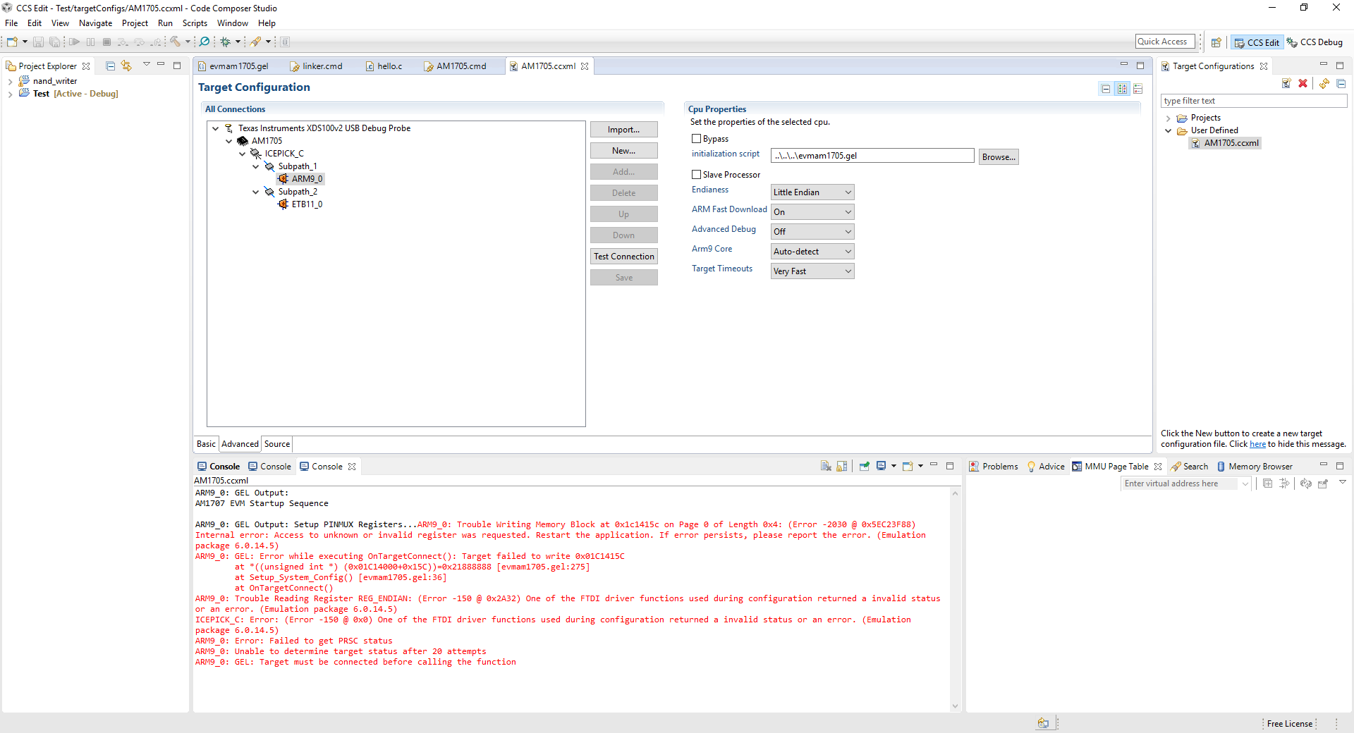
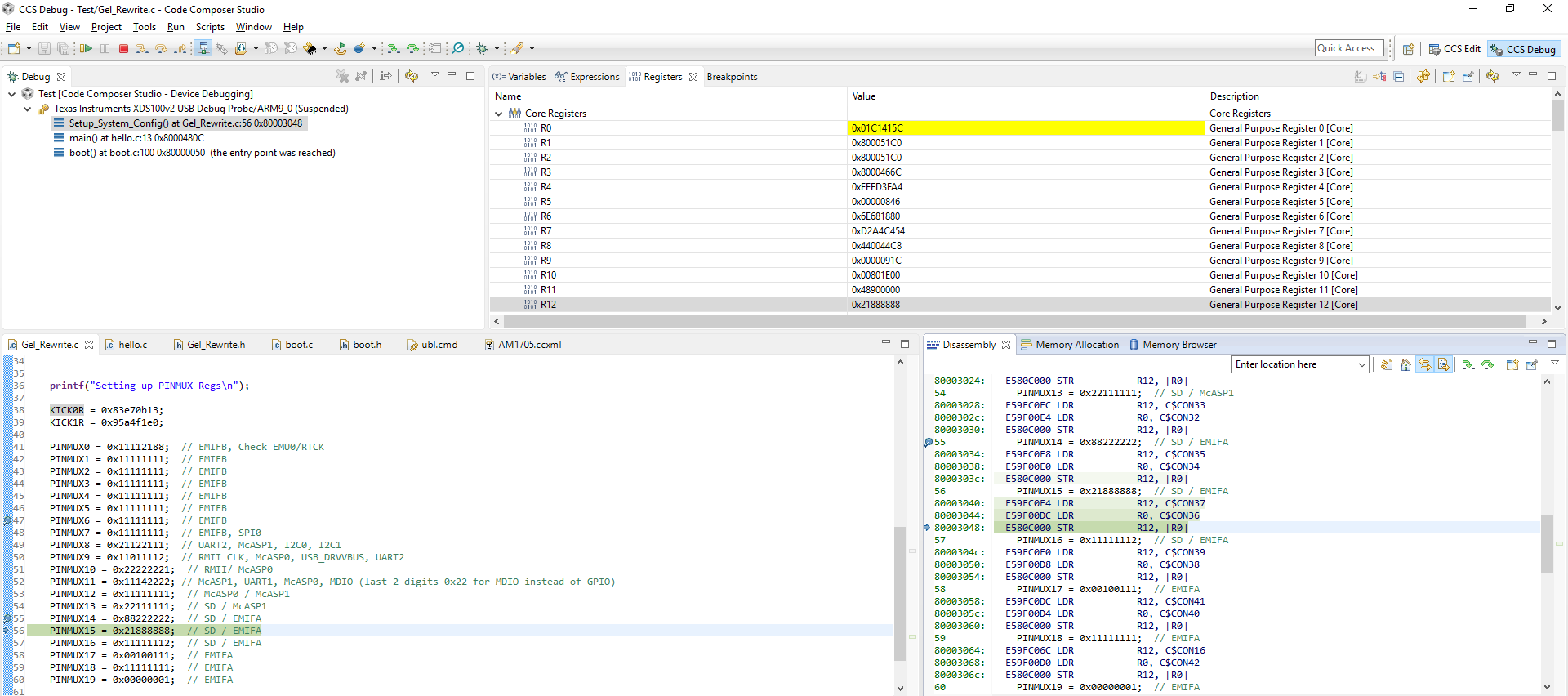
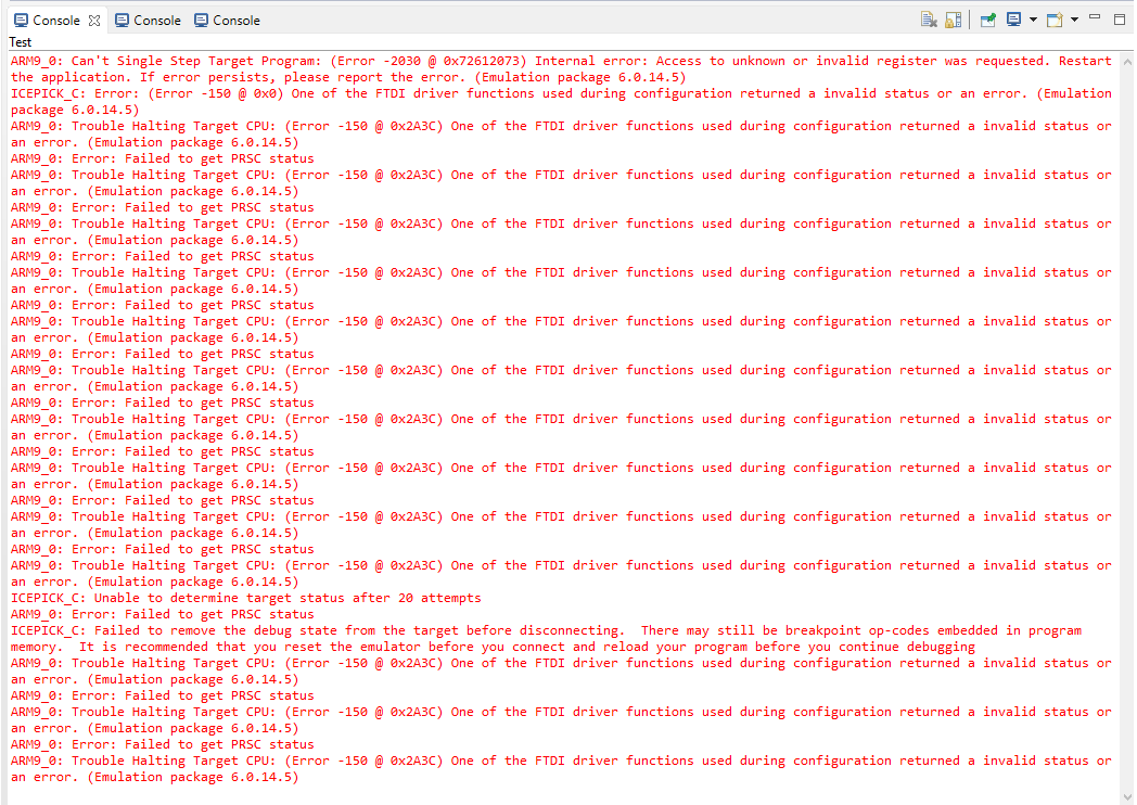
ARM9_0: Trouble Writing Memory Block at 0x1c1415c on Page 0 of Length 0x4: (Error -2030 @ 0x64703F88) Internal error: Access to unknown or invalid register was requested. Restart the application. If error persists, please report the error. (Emulation package 6.0.14.5)
ARM9_0: GEL: Error while executing OnTargetConnect(): Target failed to write 0x01C1415C
at *((unsigned int *) (0x01C14000+0x15C))=0x21888888 [evmam1705.gel:278]
at Setup_System_Config() [evmam1705.gel:39]
at OnTargetConnect()
The location it is referring to is the PINMUX15 register. When I comment out that line then it crashes on the next register but none of the ones before.
I've also used the OMAP_L1xxx debugging script and I have attached the output of Run_All.
I've already checked the soldering on the ground pad as that was an issue on another post. I'm currently running the startup script with the hello_world program that I know works.
Any hints or suggestions will be greatly appreciated.
Thanks,
Haydn
ARM9_0: GEL Output: ---------------------------------------------
ARM9_0: GEL Output: |               BOOTROM Info                |
ARM9_0: GEL Output: ---------------------------------------------
ARM9_0: GEL Output: ROM ID: d800k003
ARM9_0: GEL Output: Silicon Revision 2.0
ARM9_0: GEL Output: Boot pins: 62199
ARM9_0: GEL Output: Boot Mode: Emulation Debug (0x0000F2F7)
ARM9_0: GEL Output:
ROM Status Code: 0x00000000
Description:ARM9_0: GEL Output: No error
ARM9_0: GEL Output:
Program Counter (PC) = 0x8001469C
ARM9_0: GEL Output:
---------------------------------------------
ARM9_0: GEL Output: |             Device Information            |
ARM9_0: GEL Output: ---------------------------------------------
ARM9_0: GEL Output: DEV_INFO_00 = 0x9B7DF02F
ARM9_0: GEL Output: DEV_INFO_01 = 0x00000000
ARM9_0: GEL Output: DEV_INFO_02 = 0x0000F2F7
ARM9_0: GEL Output: DEV_INFO_03 = 0x00000012
ARM9_0: GEL Output: DEV_INFO_04 = 0x00000000
ARM9_0: GEL Output: DEV_INFO_05 = 0x000003E0
ARM9_0: GEL Output: DEV_INFO_06 = 0x00000080
ARM9_0: GEL Output: DEV_INFO_07-DEV_INFO_08-DEV_INFO_09-DEV_INFO_10-DEV_INFO_11-DEV_INFO_12 = 8-0-151387-5-8-5
ARM9_0: GEL Output: DEV_INFO_13,DEV_INFO_14,DEV_INFO_15,DEV_INFO_16 = 0,0,0,9029
ARM9_0: GEL Output: -----
ARM9_0: GEL Output: DEV_INFO_17 = 0x00030003
ARM9_0: GEL Output: DEV_INFO_18 = 0x00000000
ARM9_0: GEL Output: DEV_INFO_19 =ARM9_0: GEL Output: 0ARM9_0: GEL Output: 0ARM9_0: GEL Output: 0ARM9_0: GEL Output: 0ARM9_0: GEL Output: 0ARM9_0: GEL Output:
ARM9_0: GEL Output: -----
ARM9_0: GEL Output: DEV_INFO_20 = 0x00000000
ARM9_0: GEL Output: DEV_INFO_21 = 0x00000000
ARM9_0: GEL Output: DEV_INFO_22 = 0x30303864
ARM9_0: GEL Output: DEV_INFO_23 = 0x3330306B
ARM9_0: GEL Output: -----
ARM9_0: GEL Output: DEV_INFO_24 = 0x05005008
ARM9_0: GEL Output: DEV_INFO_25 = 0x08024F5B
ARM9_0: GEL Output: DEV_INFO_06 = 0x00000080
ARM9_0: GEL Output: DEV_INFO_26 = 0x468A0000
ARM9_0: GEL Output:

ARM9_0: GEL Output:
ARM9_0: GEL Output: ---------------------------------------------
ARM9_0: GEL Output: |              Clock Information             |
ARM9_0: GEL Output: ---------------------------------------------
ARM9_0: GEL Output:
ARM9_0: GEL Output: PLLs configured to utilize crystal.
ARM9_0: GEL Output: ASYNC3 = PLL0_SYSCLK2
ARM9_0: GEL Output:
ARM9_0: GEL Output: NOTE:  All clock frequencies in following PLL sections are based
ARM9_0: GEL Output: off OSCIN = 24 MHz.  If that value does not match your hardware
ARM9_0: GEL Output: you should change the #define in the top of the gel file, save it,
ARM9_0: GEL Output: and then reload.
ARM9_0: GEL Output:
ARM9_0: GEL Output: ---------------------------------------------
ARM9_0: GEL Output: |              PLL0 Information             |
ARM9_0: GEL Output: ---------------------------------------------
ARM9_0: GEL Output:
ARM9_0: GEL Output: PLL0_SYSCLK1 = 24 MHz
ARM9_0: GEL Output: PLL0_SYSCLK2 = 12 MHz
ARM9_0: GEL Output: PLL0_SYSCLK3 = 8 MHz
ARM9_0: GEL Output: PLL0_SYSCLK4 = 6 MHz
ARM9_0: GEL Output: PLL0_SYSCLK5 = 8 MHz
ARM9_0: GEL Output: PLL0_SYSCLK6 = 24 MHz
ARM9_0: GEL Output: PLL0_SYSCLK7 = 4 MHz
ARM9_0: GEL Output:
ARM9_0: GEL Output: ---------------------------------------------
ARM9_0: GEL Output: |              PSC0 Information             |
ARM9_0: GEL Output: ---------------------------------------------
ARM9_0: GEL Output:
ARM9_0: GEL Output: State Decoder:
ARM9_0: GEL Output:  0 = SwRstDisable (reset asserted, clock off)
ARM9_0: GEL Output:  1 = SyncReset (reset assered, clock on)
ARM9_0: GEL Output:  2 = Disable (reset de-asserted, clock off)
ARM9_0: GEL Output:  3 = Enable (reset de-asserted, clock on)
ARM9_0: GEL Output: >3 = Transition in progress
ARM9_0: GEL Output:
ARM9_0: GEL Output: Module 0:	EDMA3CC (0)        STATE = 0
ARM9_0: GEL Output: Module 1:	EDMA3 TC0          STATE = 0
ARM9_0: GEL Output: Module 2:	EDMA3 TC1          STATE = 0
ARM9_0: GEL Output: Module 3:	EMIFA (BR7)        STATE = 0
ARM9_0: GEL Output: Module 4:	SPI 0              STATE = 0
ARM9_0: GEL Output: Module 5:	MMC/SD 0           STATE = 0
ARM9_0: GEL Output: Module 6:	AINTC              STATE = 3
ARM9_0: GEL Output: Module 7:	ARM RAM/ROM        STATE = 3
ARM9_0: GEL Output: Module 9:	UART 0             STATE = 0
ARM9_0: GEL Output: Module 10:	SCR 0 (BR0/1/2/8)  STATE = 3
ARM9_0: GEL Output: Module 11:	SCR 1 (BR4)        STATE = 3
ARM9_0: GEL Output: Module 12:	SCR 2 (BR3/5/6)    STATE = 3
ARM9_0: GEL Output: Module 13:	PRUSS              STATE = 0
ARM9_0: GEL Output: Module 14:	ARM                STATE = 3
ARM9_0: GEL Output: Module 15:	DSP                STATE = 0
ARM9_0: GEL Output:
ARM9_0: GEL Output: ---------------------------------------------
ARM9_0: GEL Output: |              PSC1 Information             |
ARM9_0: GEL Output: ---------------------------------------------
ARM9_0: GEL Output:
ARM9_0: GEL Output: State Decoder:
ARM9_0: GEL Output:  0 = SwRstDisable (reset asserted, clock off)
ARM9_0: GEL Output:  1 = SyncReset (reset assered, clock on)
ARM9_0: GEL Output:  2 = Disable (reset de-asserted, clock off)
ARM9_0: GEL Output:  3 = Enable (reset de-asserted, clock on)
ARM9_0: GEL Output: >3 = Transition in progress
ARM9_0: GEL Output:
ARM9_0: GEL Output: Module 1:	USB0 (2.0)         STATE = 0
ARM9_0: GEL Output: Module 2:	USB1 (1.1)         STATE = 0
ARM9_0: GEL Output: Module 3:	GPIO               STATE = 0
ARM9_0: GEL Output: Module 4:	UHPI               STATE = 0
ARM9_0: GEL Output: Module 5:	EMAC               STATE = 0
ARM9_0: GEL Output: Module 6:	EMIFB (BR20)       STATE = 0
ARM9_0: GEL Output: Module 7:	MCASP0 + FIFO      STATE = 0
ARM9_0: GEL Output: Module 8:	MCASP1 + FIFO      STATE = 0
ARM9_0: GEL Output: Module 9:	MCASP2 + FIFO      STATE = 0
ARM9_0: GEL Output: Module 10:	SPI 1              STATE = 0
ARM9_0: GEL Output: Module 11:	I2C 1              STATE = 0
ARM9_0: GEL Output: Module 12:	UART 1             STATE = 0
ARM9_0: GEL Output: Module 13:	UART 2             STATE = 0
ARM9_0: GEL Output: Module 16:	LCDC               STATE = 0
ARM9_0: GEL Output: Module 17:	eHRPWM (all)       STATE = 0
ARM9_0: GEL Output: Module 20:	eCAP (all)         STATE = 0
ARM9_0: GEL Output: Module 21:	eQEP 0/1           STATE = 0
ARM9_0: GEL Output: Module 24:	SCR8 (Br15)        STATE = 3
ARM9_0: GEL Output: Module 25:	SCR7 (Br12)        STATE = 3
ARM9_0: GEL Output: Module 26:	SCR12 (Br18)       STATE = 3
ARM9_0: GEL Output: Module 31:	L3 RAM (Br13)      STATE = 3


