


I use the attateched sample_ini.ini file to make the ais file of a simple application and successfully do secure boot from nandflash.
But I didn't understand how to caculate the PLLandConfig settings in the ini file.
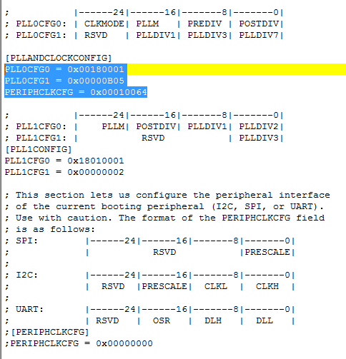
As in the configuration in sample_ini.ini file:
Q1: How to caclulate the UART baudrate?
Since the crystal is 24MHz, I caculated the sysclks as shown in the following table.
|
crystal |
*1 |
24MHz |
|
|
PLL0_SYSCLK1 |
*24/2/1=*12 |
288MHz |
|
|
PLL0_SYSCLK3 |
*24/2/12=*1 |
24MHz |
|
|
PLL0_SYSCLK7 |
*24/2/6=*2 |
48MHz |
|
|
PLL1_SYSCLK1 |
*24/2/1=*12 |
288MHz |
|
|
PLL1_SYSCLK2 |
*24/2/2=*6 |
144MHz |
|
|
PLL1_SYSCLK3 |
*24/2/3=*4 |
92MHz |
|
According to the C6748 Technical Reference, "The ASYNC3 modules use PLL0_SYSCLK2 by default, but all these modules can be configured as a group to use
PLL1_SYSCLK2 by programming the ASYNC3_CLKSRC bit in the chip configuration 3 register (CFGCHIP3) of the system
configuration (SYSCFG) module."
I didn't find any setting of ASYNC3_CLKSRC in the sample_ini.ini file. But I think here, UART Input Clock=PLL1_SYSCLK2.
Since OSR=0x01, DLH=0x00, DLL=0x64
So, UART BaudRate=144MHz/13/100=110,769Hz , which is quite far from 115,200Hz.
What's wrong with my caculation?
Thank you.https://e2e.ti.com/cfs-file/__key/communityserver-discussions-components-files/791/8637.sample_5F00_ini.ini
Frank

