This thread has been locked.

If you have a related question, please click the "Ask a related question" button in the top right corner. The newly created question will be automatically linked to this question.

EDMA vs QDMA submit performance


Hello!

I'd like to ask for advice on the following topic. In our system we use C6414 DSP. It is connected to FPGA through EMIFA in 64-bit mode. We have to move OFDM data to and from FPGA at a rate about 2 to 4 times per approx. 100 us. We were using regular REG_WRITE/REG_READ to do the job. Obviously, that consumes most of DSP time. One 2KB transfer takes about 17 us. Now I'm trying to use EDMA mechanism to do that. Because I have to swap left/right side data when downloading to FPGA buffer, I use chaining of EDMA transfers. To reduce number of required operations, all necessary channels are configured in advance. Then, on FPGA interrupt I only issue EDMA_setChannel() for right side data. On completion in initiates chained left side transfer.

To monitor performance I use the following mechanism. In FPGA there is a test point register. I just write/clear certain bit and monitor it with oscilloscope.

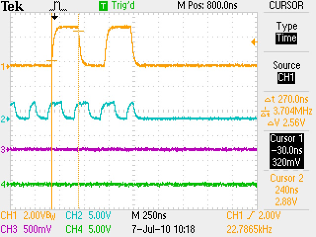
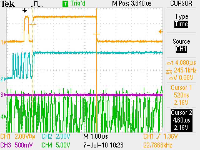
So my observation is that It takes about 17 us to transfer 2KB block. I monitor that by CE signal on FPGA. In the same time, submitting EDMA transfer takes 4.4 us. Namely, this piece of code

SET_TP(TX_OFDM_TP);                 // Set test point High
EDMA_setChannel(dma->hdl_tx_ch1_r); // Trigger event
CLR_TP(TX_OFDM_TP);                 // Clear test point

takes 4.4 us to execute. It definitely much better, but I wonder, why so long.

Also I've tried to use QDMA for right side transfer and chain EDMA transfer to left side data like this:

SET_TP(TX_OFDM_TP);                  // Set test point High
EDMA_qdmaConfig(&dma->cfg_tx_ch1_r); // Setup QDMA
CLR_TP(TX_OFDM_TP);                  // Clear test point

But it takes same 4.4 us to submit. I even manually set up QDMA registers - with same result.

So I wonder, why it takes so long time for what was claimed to take "only one to five CPU cycles" according to spru234. I was suspecting big overhead of EMIFA access for test point writes, so I've tried

SET_TP(TX_OFDM_TP);  // Set test point High
x = y;               // Some minor stuff
CLR_TP(TX_OFDM_TP);  // Clear test point

and it took only 260 ns. So it looks that configuring EDMA/QDMA itself takes that long time.

Just in case it that might be important. In our configuration we don't use L2 cache. All L2 memory is split in SRAM and heap.

Would appreciate any advice. Thanks in advance.

  • I may ask more questions than offer answers right now, but you are definitely going the right direction. Using the EDMA instead of DSP MIPS is exactly what the EDMA is intended for. And I completely agree that 4.4us sounds like way too much time for the execution of EDMA_setChannel().

    It was a good test to use "x = y;". I would even suggest trying it with just

    suggested calibration said:
    SET_TP(TX_OFDM_TP);  // Set test point High
    CLR_TP(TX_OFDM_TP);  // Clear test point
    SET_TP(TX_OFDM_TP);  // Set test point High
    CLR_TP(TX_OFDM_TP);  // Clear test point

    The reason for the double pulse is to eliminate possible read/write interference.

    Are all program and data in L2, or at least the code that is executed in the tests and the struct to which 'dma' points? And SET_TP/CLR_TP?

    suggested test said:
    SET_TP(TX_OFDM_TP);  // Set test point High
    x = EDMA_RGET(ESRL); // dummy config bus read
    CLR_TP(TX_OFDM_TP);  // Clear test point
    SET_TP(TX_OFDM_TP);  // Set test point High
    EDMA_setChannel(dma->hdl_tx_ch1_r); // Trigger event
    CLR_TP(TX_OFDM_TP);  // Clear test point

    The idea is to make sure the config bus is cleared before EDMA_setChannel gets called.

    Are you using the optimizer at all? If not, please use at least -o1 and see what it does to the performance.

  • First of all, thank you very much for the help.

    To make things clear.

    I use -o1 optimization level, but no program level optimization.

    Whole program code and data reside in L2, no other memories used.

    SET_TP is in fact

    #define SET_TP(pin)  REG_WRITE(TP_REG_ADDR_FPGA, REG_READ64(TP_REG_ADDR_FPGA)  | (1 << pin))

    FPGA addresses are on EMIFA CE2 address space.

    suggested calibration said:
    SET_TP(TX_OFDM_TP);  // Set test point High

    CLR_TP(TX_OFDM_TP);  // Clear test point
    SET_TP(TX_OFDM_TP);  // Set test point High
    CLR_TP(TX_OFDM_TP);  // Clear test point

    Here is a picture from the scope:

    Topmost yellow line is test point.

    For next test

    suggested test said:
    SET_TP(TX_OFDM_TP);  // Set test point High
    x = EDMA_RGET(ESRL); // dummy config bus read
    CLR_TP(TX_OFDM_TP);  // Clear test point
    SET_TP(TX_OFDM_TP);  // Set test point High
    EDMA_setChannel(dma->hdl_tx_ch1_r); // Trigger event
    CLR_TP(TX_OFDM_TP);  // Clear test point

    picture is

    Here again topmost yellow line is test point. Second blue line is CE signal of FPGA. Several CE strobes before test point high first time are FPGA interrupt register read and clear. But now seems I know the reason for delay. I think, that immediately after EDMA_setChannel EDMA controller starts the transfer. So our attempt to CLR_TP(TX_OFDM_TP); will compete with this transfer.

    I have also noticed, that set/clear test point sequence happens faster during read transfer. On the following picture odd strobes correspond to read setup and even strobes are for write setup. Former ones are of 2.8 us and latter - 4.4 us.

    So I guess, my approach to benchmark using FPGA test point was wrong. Could you please comment on this? Could you please suggest some better test to verify timing and performance?

    Thanks in advance.

  • The one to five CPU cycle refers to how QDMA respond to the triggering command. However, for DSP to issue those commands, it needs to go through some chip level interconnection, which adds the latency. What you see is probabliy due to those latency at the chip level.But 260ns seems too high. What kind of speed do you run on C6414?

    Regards,


    Chunhua

  • CPU Core is clocked @720 MHz. EMIFA, through which we connect to FPGA, is clocked @1/8, that is 90 MHz.

  • rrlagic said:
    I have also noticed, that set/clear test point sequence happens faster during read transfer.

    What does this mean, "read transfer"? I think I understand that the write transfer means writing to ESR to start the DMA transfer and that you believe the DMA transfer to the FPGA is holding off the length of the test point pulse. Is the read transfer one in which you are reading from the FPGA and the write transfer is when you write to the FPGA?

    rrlagic said:
    topmost yellow line is test point. Second blue line is CE signal of FPGA.

    Looking at the blue line, I would have expected it to be low during the DMA transfers to the FPGA. Is there a different CE used for these DMA transfers? Is this the same CE that is used for the TP macros to read/modify/write the TP register in the FPGA?

    rrlagic said:
    Could you please suggest some better test to verify timing and performance?

    If you can use some other pin on the DSP as a GPIO, like an unused timer pin or serial port pin, that would avoid any conflict with the EMIF going to the FPGA. Or if you have a timer that could be read before and after the function call, instead of the SET_TP/CLR_TP macros, you could get a measurement of the time it takes to make the function call and return.

  • RandyP said:

    What does this mean, "read transfer"? I think I understand that the write transfer means writing to ESR to start the DMA transfer and that you believe the DMA transfer to the FPGA is holding off the length of the test point pulse. Is the read transfer one in which you are reading from the FPGA and the write transfer is when you write to the FPGA?

    The latter one is correct: I mean write transfer when EDMA writes to FPGA and read transfer when EDMA reads from FPGA.

    RandyP said:

    Looking at the blue line, I would have expected it to be low during the DMA transfers to the FPGA. Is there a different CE used for these DMA transfers? Is this the same CE that is used for the TP macros to read/modify/write the TP register in the FPGA?

    DSP's EMIFA CE signal gets inverted inside of FPGA. In fact, this is inverse if EMIFA CE2 signal. And yes, FPGA buffer read and test point manipulations are on same CE. Inside of FPGA we decode address bus to access specific registers or buffers.

    RandyP said:

    If you can use some other pin on the DSP as a GPIO, like an unused timer pin or serial port pin, that would avoid any conflict with the EMIF going to the FPGA. Or if you have a timer that could be read before and after the function call, instead of the SET_TP/CLR_TP macros, you could get a measurement of the time it takes to make the function call and return.

    O, good hint. I have timer running for handmade clock (not DSP/BIOS clock), so I think, I can read its counter value for benchmark. Thanks again :-)