This thread has been locked.
If you have a related question, please click the "Ask a related question" button in the top right corner. The newly created question will be automatically linked to this question.
Dear,
I am working on AM4378 project and it is based on AM437x-gp-evm. I built sitara linux and boot from SD card now. It is working fine.
Now I wanted to transfer all linux files(MLO, uboot.img, kernel, file system, etc) to eMMC and boot it from eMMC. How do i achieve this?
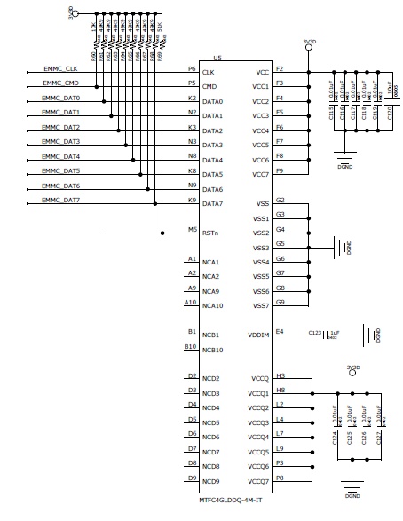
My schematic is as follows
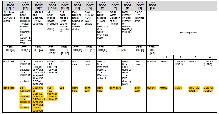
My boot sequence given below.
I am following the below link to update files and boot from eMMC,
I enter the following command from uboot,
U-Boot # printenv partitions uuid_disk=${uuid_gpt_disk};name=rootfs,start=2MiB,size=-,uuid=${uuid_gpt_rootfs} U-Boot # setenv uuid_gpt_disk ...first uuid... U-Boot # setenv uuid_gpt_rootfs ...second uuid... U-Boot # gpt write mmc 1 ${partitions}
When i enter "U-Boot # gpt write mmc 1 ${partitions} " , I got below error,
"Card did not respond to voltage select!
do_gpt: mmc dev 1 NOT available "
What could be the reason? How do i solve this problem?
Regards,
Winiston.P
Hi,
Can you try executing:
mmc rescan
mmc info
from u-boot prompt?
If you get the same errors with these commands, please add CONFIG_MMC_TRACE & DEBUG, to enable a more verbose u-boot log & share your serial console output.
Best Regards,
Yordan
Dear Yordan,
I executed the commands you said. I did not get any error messages. Please see my serial console output
U-Boot# mmc rescan
17: mmc rescan
U-Boot# mmc info
23: mmc info
Device: OMAP SD/MMC
Manufacturer ID: 74
OEM: 4a60
Name: USDU1
Tran Speed: 50000000
Rd Block Len: 512
SD version 3.0
High Capacity: Yes
Capacity: 15 GiB
Bus Width: 4-bit
Erase Group Size: 512 Bytes
U-Boot#
Regards,
Winiston.P
Dear Yordan,
I am waiting for your reply to solve this issue.
Regards,
Winiston.P
Dear Yordan,
I executed the commands you said. I did not get any error messages. Please see my serial console output
U-Boot# mmc rescan
17: mmc rescan
U-Boot# mmc info
23: mmc info
Device: OMAP SD/MMC
Manufacturer ID: 74
OEM: 4a60
Name: USDU1
Tran Speed: 50000000
Rd Block Len: 512
SD version 3.0
High Capacity: Yes
Capacity: 15 GiB
Bus Width: 4-bit
Erase Group Size: 512 Bytes
U-Boot#
I am waiting for your reply for long time... Please let me know if you need any console output from my side.
Regards,
Winiston.P
Dear Yordan,
1. I can not switch to MMC1(emmc). If i enter " U-Boot # mmc dev 1", it gives below error,
"mmc dev 1
Card did not respond to voltage select! "
Is it a conflict in voltage?
Note:I am using 3.3v bank for emmc.
If i enter "mmc rescan & mmc info ", It gives, MMC0(sd card) information only.
2. My pinmux settings seems to be correct. Please find attached dts file for your reference.
/* This file was auto-generated by TI PinMux on 22-07-2016 at 15:43:54. */ /* This file should only be used as a reference. Some pins/peripherals, */ /* depending on your use case, may need additional configuration. */ /* Some or all the pins from the following groups are not used by device tree myrtc1 usb_otg usb_host myadc1 ram */ /dts-v1/; #include "am4372.dtsi" #include <dt-bindings/pinctrl/am43xx.h> #include <dt-bindings/pwm/pwm.h> #include <dt-bindings/gpio/gpio.h> / { model = "TI AM437x GP EVM"; compatible = "ti,am437x-gp-evm","ti,am4372","ti,am43"; aliases { display0 = &lcd0; serial3 = &uart3; }; evm_v3_3d: fixedregulator-v3_3d { compatible = "regulator-fixed"; regulator-name = "evm_v3_3d"; regulator-min-microvolt = <3300000>; regulator-max-microvolt = <3300000>; enable-active-high; }; vtt_fixed: fixedregulator-vtt { compatible = "regulator-fixed"; regulator-name = "vtt_fixed"; regulator-min-microvolt = <1500000>; regulator-max-microvolt = <1500000>; regulator-always-on; regulator-boot-on; enable-active-high; gpio = <&gpio2 1 GPIO_ACTIVE_HIGH>; }; vmmcwl_fixed: fixedregulator-mmcwl { compatible = "regulator-fixed"; regulator-name = "vmmcwl_fixed"; regulator-min-microvolt = <1800000>; regulator-max-microvolt = <1800000>; /*belowlines added by wini */ startup-delay-us = <70000>; /* WLAN_EN GPIO for this board - Bank0, pin18 */ gpio = <&gpio0 18 GPIO_ACTIVE_HIGH>; enable-active-high; }; lcd_bl: backlight { compatible = "pwm-backlight"; pwms = <&ecap0 0 50000 PWM_POLARITY_INVERTED>; brightness-levels = <0 51 53 56 62 75 101 152 255>; default-brightness-level = <8>; }; lcd0: display { compatible = "panel-dpi"; label = "lcd"; panel-timing { clock-frequency = <25000000>; hactive = <640>; vactive = <480>; hfront-porch = <12>; hback-porch = <52>; hsync-len = <96>; vback-porch = <31>; vfront-porch = <11>; vsync-len = <2>; hsync-active = <0>; vsync-active = <0>; de-active = <1>; pixelclk-active = <1>; }; port { lcd_in: endpoint { remote-endpoint = <&dpi_out>; }; }; }; /*below lines added by wini */ /* fixed 12MHz oscillator */ refclk: oscillator { #clock-cells = <0>; compatible = "fixed-clock"; clock-frequency = <12000000>; }; /* fixed 32k external oscillator clock */ clk_32k_rtc: clk_32k_rtc { #clock-cells = <0>; compatible = "fixed-clock"; clock-frequency = <32768>; }; sound0: sound@0 { compatible = "simple-audio-card"; simple-audio-card,name = "AM437x-GP-EVM"; simple-audio-card,widgets = "Headphone", "Headphone Jack", "Microphone", "Microphone Jack", "Speaker", "External Speaker"; simple-audio-card,routing = "Headphone Jack", "HPLOUT", "Headphone Jack", "HPROUT", "MIC3L", "Microphone Jack", "MIC3R", "Microphone Jack", "External Speaker", "MONO_LOUT"; simple-audio-card,format = "dsp_b"; simple-audio-card,bitclock-master = <&sound0_master>; simple-audio-card,frame-master = <&sound0_master>; simple-audio-card,bitclock-inversion; simple-audio-card,cpu { sound-dai = <&mcasp1>; system-clock-frequency = <12000000>; }; sound0_master: simple-audio-card,codec { sound-dai = <&tlv320aic3106>; system-clock-frequency = <12000000>; }; }; audio_mstrclk: mclk_osc { compatible = "fixed-clock"; #clock-cells = <0>; clock-frequency = <12000000>; }; }; &am43xx_pinmux { pinctrl-names = "default", "sleep"; /* modified by wini */ pinctrl-0 = <&wlan_irq_pins_default &ddr3_vtt_toggle_default &debugss_pins>; /* added by wini */ pinctrl-1 = <&wlan_irq_pins_sleep>; ddr3_vtt_toggle_default: ddr_vtt_toggle_default { pinctrl-single,pins = < 0x8C (DS0_PULL_UP_DOWN_EN | PIN_OUTPUT_PULLUP | DS0_FORCE_OFF_MODE | MUX_MODE7) /* (A12) gpmc_clk.gpio2[1] */ >; }; i2c0_pins: i2c0_pins { pinctrl-single,pins = < 0x18c (PIN_INPUT_PULLUP | SLEWCTRL_FAST | MUX_MODE0) /* (Y22) i2c0_scl.i2c0_scl */ 0x188 (PIN_INPUT_PULLUP | SLEWCTRL_FAST | MUX_MODE0) /* (AB24) i2c0_sda.i2c0_sda */ >; }; i2c1_pins_default: i2c1_pins_default { pinctrl-single,pins = < 0x240 (PIN_INPUT_PULLUP | SLEWCTRL_FAST | MUX_MODE1) /* (G20) gpio5_10.I2C1_SCL */ 0x248 (PIN_INPUT_PULLUP | SLEWCTRL_FAST | MUX_MODE1) /* (E25) gpio5_12.I2C1_SDA */ >; }; sd_card_pins_default: sd_card_pins_default { pinctrl-single,pins = < 0x100 (PIN_INPUT_PULLUP | MUX_MODE0 ) /* (D1) mmc0_clk.mmc0_clk */ 0x104 (PIN_INPUT_PULLUP | MUX_MODE0 ) /* (D2) mmc0_cmd.mmc0_cmd */ 0xfc (PIN_INPUT_PULLUP | MUX_MODE0 ) /* (C1) mmc0_dat0.mmc0_dat0 */ 0xf8 (PIN_INPUT_PULLUP | MUX_MODE0 ) /* (C2) mmc0_dat1.mmc0_dat1 */ 0xf4 (PIN_INPUT_PULLUP | MUX_MODE0 ) /* (B2) mmc0_dat2.mmc0_dat2 */ 0xf0 (PIN_INPUT_PULLUP | MUX_MODE0 ) /* (B1) mmc0_dat3.mmc0_dat3 */ 0x160 (PIN_INPUT_PULLUP | MUX_MODE5 ) /* (R25) spi0_cs1.mmc0_sdcd */ >; }; /* Optional sleep pin settings. Must manually enter values in the below skeleton. */ sd_card_pins_sleep: sd_card_pins_sleep { pinctrl-single,pins = < 0x100 (PIN_INPUT_PULLDOWN | MUX_MODE7 ) /* (D1) mmc0_clk.mmc0_clk */ 0x104 (PIN_INPUT | PULL_DISABLE | MUX_MODE7 ) /* (D2) mmc0_cmd.mmc0_cmd */ 0xfc (PIN_INPUT | PULL_DISABLE | MUX_MODE7 ) /* (C1) mmc0_dat0.mmc0_dat0 */ 0xf8 (PIN_INPUT | PULL_DISABLE | MUX_MODE7 ) /* (C2) mmc0_dat1.mmc0_dat1 */ 0xf4 (PIN_INPUT | PULL_DISABLE | MUX_MODE7 ) /* (B2) mmc0_dat2.mmc0_dat2 */ 0xf0 (PIN_INPUT | PULL_DISABLE | MUX_MODE7 ) /* (B1) mmc0_dat3.mmc0_dat3 */ 0x160 (PIN_INPUT | PULL_DISABLE | MUX_MODE7 ) /* (R25) spi0_cs1.mmc0_sdcd */ >; }; emmc_pins_default: emmc_pins_default { pinctrl-single,pins = < 0x80 (PIN_INPUT_PULLUP | MUX_MODE2 ) /* (B9) gpmc_csn1.mmc1_clk */ 0x84 (PIN_INPUT_PULLUP | MUX_MODE2 ) /* (F10) gpmc_csn2.mmc1_cmd */ 0x20 (PIN_INPUT_PULLUP | MUX_MODE2 ) /* (B10) gpmc_ad8.mmc1_dat0 */ 0x24 (PIN_INPUT_PULLUP | MUX_MODE2 ) /* (A10) gpmc_ad9.mmc1_dat1 */ 0x28 (PIN_INPUT_PULLUP | MUX_MODE2 ) /* (F11) gpmc_ad10.mmc1_dat2 */ 0x2c (PIN_INPUT_PULLUP | MUX_MODE2 ) /* (D11) gpmc_ad11.mmc1_dat3 */ 0x30 (PIN_INPUT_PULLUP | MUX_MODE2 ) /* (E11) gpmc_ad12.mmc1_dat4 */ 0x34 (PIN_INPUT_PULLUP | MUX_MODE2 ) /* (C11) gpmc_ad13.mmc1_dat5 */ 0x38 (PIN_INPUT_PULLUP | MUX_MODE2 ) /* (B11) gpmc_ad14.mmc1_dat6 */ 0x3c (PIN_INPUT_PULLUP | MUX_MODE2 ) /* (A11) gpmc_ad15.mmc1_dat7 */ >; }; /* Optional sleep pin settings. Must manually enter values in the below skeleton. */ emmc_pins_sleep: emmc_pins_sleep { pinctrl-single,pins = < 0x80 (PIN_INPUT_PULLDOWN | MUX_MODE7 ) /* (B9) gpmc_csn1.mmc1_clk */ 0x84 (PIN_INPUT_PULLDOWN | MUX_MODE7 ) /* (F10) gpmc_csn2.mmc1_cmd */ 0x20 (PIN_INPUT_PULLDOWN | MUX_MODE7 ) /* (B10) gpmc_ad8.mmc1_dat0 */ 0x24 (PIN_INPUT_PULLDOWN | MUX_MODE7 ) /* (A10) gpmc_ad9.mmc1_dat1 */ 0x28 (PIN_INPUT_PULLDOWN | MUX_MODE7 ) /* (F11) gpmc_ad10.mmc1_dat2 */ 0x2c (PIN_INPUT_PULLDOWN | MUX_MODE7 ) /* (D11) gpmc_ad11.mmc1_dat3 */ 0x30 (PIN_INPUT_PULLDOWN | MUX_MODE7 ) /* (E11) gpmc_ad12.mmc1_dat4 */ 0x34 (PIN_INPUT_PULLDOWN | MUX_MODE7 ) /* (C11) gpmc_ad13.mmc1_dat5 */ 0x38 (PIN_INPUT_PULLDOWN | MUX_MODE7 ) /* (B11) gpmc_ad14.mmc1_dat6 */ 0x3c (PIN_INPUT_PULLDOWN | MUX_MODE7 ) /* (A11) gpmc_ad15.mmc1_dat7 */ >; }; ecap0_pins_default: backlight_pins_default { pinctrl-single,pins = < 0x164 MUX_MODE0 /* (G24) eCAP0_in_PWM0_out.eCAP0_in_PWM0_out MODE0 */ >; }; ecap0_pins_sleep: backlight_pins_sleep { pinctrl-single,pins = < 0x164 (PIN_INPUT_PULLDOWN | MUX_MODE7) >; }; cpsw_default: cpsw_default { pinctrl-single,pins = < 0x40 (PIN_OUTPUT_PULLDOWN | MUX_MODE2 ) /* (C3) gpmc_a0.rgmii2_tctl */ 0x44 (PIN_INPUT_PULLDOWN | MUX_MODE2 ) /* (C5) gpmc_a1.rgmii2_rctl */ 0x58 (PIN_OUTPUT_PULLDOWN | MUX_MODE2 ) /* (E8) gpmc_a6.rgmii2_tclk */ 0x5c (PIN_INPUT_PULLDOWN | MUX_MODE2 ) /* (F6) gpmc_a7.rgmii2_rclk */ 0x54 (PIN_OUTPUT_PULLDOWN | MUX_MODE2 ) /* (E7) gpmc_a5.rgmii2_td0 */ 0x50 (PIN_OUTPUT_PULLDOWN | MUX_MODE2 ) /* (D7) gpmc_a4.rgmii2_td1 */ 0x4c (PIN_OUTPUT_PULLDOWN | MUX_MODE2 ) /* (A4) gpmc_a3.rgmii2_td2 */ 0x48 (PIN_OUTPUT_PULLDOWN | MUX_MODE2 ) /* (C6) gpmc_a2.rgmii2_td3 */ 0x6c (PIN_INPUT_PULLDOWN | MUX_MODE2 ) /* (D8) gpmc_a11.rgmii2_rd0 */ 0x68 (PIN_INPUT_PULLDOWN | MUX_MODE2 ) /* (G8) gpmc_a10.rgmii2_rd1 */ 0x64 (PIN_INPUT_PULLDOWN | MUX_MODE2 ) /* (B4) gpmc_a9.rgmii2_rd2 */ 0x60 (PIN_INPUT_PULLDOWN | MUX_MODE2 ) /* (F7) gpmc_a8.rgmii2_rd3 */ >; }; /* Optional sleep pin settings. Must manually enter values in the below skeleton. */ cpsw_sleep: cpsw_sleep { pinctrl-single,pins = < 0x40 (PIN_INPUT_PULLDOWN | MUX_MODE7 ) /* (C3) gpmc_a0.rgmii2_tctl */ 0x44 (PIN_INPUT_PULLDOWN | MUX_MODE7 ) /* (C5) gpmc_a1.rgmii2_rctl */ 0x58 (PIN_INPUT_PULLDOWN | MUX_MODE7 ) /* (E8) gpmc_a6.rgmii2_tclk */ 0x5c (PIN_INPUT_PULLDOWN | MUX_MODE7 ) /* (F6) gpmc_a7.rgmii2_rclk */ 0x54 (PIN_INPUT_PULLDOWN | MUX_MODE7 ) /* (E7) gpmc_a5.rgmii2_td0 */ 0x50 (PIN_INPUT_PULLDOWN | MUX_MODE7 ) /* (D7) gpmc_a4.rgmii2_td1 */ 0x4c (PIN_INPUT_PULLDOWN | MUX_MODE7 ) /* (A4) gpmc_a3.rgmii2_td2 */ 0x48 (PIN_INPUT_PULLDOWN | MUX_MODE7 ) /* (C6) gpmc_a2.rgmii2_td3 */ 0x6c (PIN_INPUT | PULL_DISABLE | MUX_MODE7 ) /* (D8) gpmc_a11.rgmii2_rd0 */ 0x68 (PIN_INPUT | PULL_DISABLE | MUX_MODE7 ) /* (G8) gpmc_a10.rgmii2_rd1 */ 0x64 (PIN_INPUT | PULL_DISABLE | MUX_MODE7 ) /* (B4) gpmc_a9.rgmii2_rd2 */ 0x60 (PIN_INPUT | PULL_DISABLE | MUX_MODE7 ) /* (F7) gpmc_a8.rgmii2_rd3 */ >; }; davinci_mdio_default: davinci_mdio_default { pinctrl-single,pins = < 0x148 (PIN_INPUT_PULLUP | SLEWCTRL_FAST | MUX_MODE0) /* (A17) mdio_data.mdio_data */ 0x14c (PIN_OUTPUT_PULLUP | MUX_MODE0) /* (B17) mdio_clk.mdio_clk */ >; }; /* Optional sleep pin settings. Must manually enter values in the below skeleton. */ davinci_mdio_sleep: davinci_mdio_sleep { pinctrl-single,pins = < 0x148 (PIN_INPUT | PULL_DISABLE | MUX_MODE7 ) /* (A17) mdio_data.mdio_data */ 0x14c (PIN_INPUT | PULL_DISABLE | MUX_MODE7 ) /* (B17) mdio_clk.mdio_clk */ >; }; /* below wlan irq definition added by wini */ wlan_irq_pins_default: wlan_irq_pins_default { pinctrl-single,pins = < 0x1a0 ( PIN_OUTPUT_PULLUP | MUX_MODE9 ) /* () gmc_a4.gpio0_18 wlan */ 0x140 ( PIN_INPUT | WAKEUP_ENABLE | MUX_MODE7 ) /* (F17) mii1_rxd0.rgmii1_rd0 */ >; }; /* Optional sleep pin settings. Must manually enter values in the below skeleton. */ wlan_irq_pins_sleep: wlan_irq_pins_sleep { pinctrl-single,pins = < 0x1a0 ( PIN_OUTPUT_PULLUP | MUX_MODE9 ) /* () gmc_a4.gpio0_18 wl_en */ 0x140 (PIN_INPUT | WAKEUP_ENABLE | MUX_MODE7 ) /* (F17) mii1_rxd0.rgmii1_rd0 */ >; }; dss_pinctrl_default: dss_pinctrl_default { pinctrl-single,pins = < 0xe0 (PIN_OUTPUT_PULLUP | MUX_MODE0 ) /* (B23) dss_vsync.dss_vsync */ 0xe4 (PIN_OUTPUT_PULLUP | MUX_MODE0 ) /* (A23) dss_hsync.dss_hsync */ 0xe8 (PIN_OUTPUT_PULLUP | MUX_MODE0 ) /* (A22) dss_pclk.dss_pclk */ 0xec (PIN_OUTPUT_PULLUP | MUX_MODE0 ) /* (A24) dss_ac_bias_en.dss_ac_bias_en */ 0xa0 (PIN_OUTPUT_PULLUP | MUX_MODE0 ) /* (B22) dss_data0.dss_data0 */ 0xa4 (PIN_OUTPUT_PULLUP | MUX_MODE0 ) /* (A21) dss_data1.dss_data1 */ 0xa8 (PIN_OUTPUT_PULLUP | MUX_MODE0 ) /* (B21) dss_data2.dss_data2 */ 0xac (PIN_OUTPUT_PULLUP | MUX_MODE0 ) /* (C21) dss_data3.dss_data3 */ 0xb0 (PIN_OUTPUT_PULLUP | MUX_MODE0 ) /* (A20) dss_data4.dss_data4 */ 0xb4 (PIN_OUTPUT_PULLUP | MUX_MODE0 ) /* (B20) dss_data5.dss_data5 */ 0xb8 (PIN_OUTPUT_PULLUP | MUX_MODE0 ) /* (C20) dss_data6.dss_data6 */ 0xbc (PIN_OUTPUT_PULLUP | MUX_MODE0 ) /* (E19) dss_data7.dss_data7 */ 0xc0 (PIN_OUTPUT_PULLUP | MUX_MODE0 ) /* (A19) dss_data8.dss_data8 */ 0xc4 (PIN_OUTPUT_PULLUP | MUX_MODE0 ) /* (B19) dss_data9.dss_data9 */ 0xc8 (PIN_OUTPUT_PULLUP | MUX_MODE0 ) /* (A18) dss_data10.dss_data10 */ 0xcc (PIN_OUTPUT_PULLUP | MUX_MODE0 ) /* (B18) dss_data11.dss_data11 */ 0xd0 (PIN_OUTPUT_PULLUP | MUX_MODE0 ) /* (C19) dss_data12.dss_data12 */ 0xd4 (PIN_OUTPUT_PULLUP | MUX_MODE0 ) /* (D19) dss_data13.dss_data13 */ 0xd8 (PIN_OUTPUT_PULLUP | MUX_MODE0 ) /* (C17) dss_data14.dss_data14 */ 0xdc (PIN_OUTPUT_PULLUP | MUX_MODE0 ) /* (D17) dss_data15.dss_data15 */ 0x1cc (PIN_OUTPUT_PULLUP | MUX_MODE2 ) /* (AC24) cam1_data9.dss_data16 */ 0x1c8 (PIN_OUTPUT_PULLUP | MUX_MODE2 ) /* (AA19) cam0_data9.dss_data17 */ 0x1c4 (PIN_OUTPUT_PULLUP | MUX_MODE2 ) /* (AB19) cam0_data8.dss_data18 */ 0x1c0 (PIN_OUTPUT_PULLUP | MUX_MODE2 ) /* (AC20) cam0_pclk.dss_data19 */ 0x1bc (PIN_OUTPUT_PULLUP | MUX_MODE2 ) /* (AD17) cam0_wen.dss_data20 */ 0x1b8 (PIN_OUTPUT_PULLUP | MUX_MODE2 ) /* (AC18) cam0_field.dss_data21 */ 0x1b4 (PIN_OUTPUT_PULLUP | MUX_MODE2 ) /* (AD18) cam0_vd.dss_data22 */ 0x1b0 (PIN_OUTPUT_PULLUP | MUX_MODE2 ) /* (AE17) cam0_hd.dss_data23 */ >; }; /* Optional sleep pin settings. Must manually enter values in the below skeleton. */ dss_pinctrl_sleep: dss_pinctrl_sleep { pinctrl-single,pins = < 0xe0 (DS0_PULL_UP_DOWN_EN | PIN_INPUT_PULLDOWN | MUX_MODE7 ) /* (B23) dss_vsync.dss_vsync */ 0xe4 (DS0_PULL_UP_DOWN_EN | PIN_INPUT_PULLDOWN | MUX_MODE7 ) /* (A23) dss_hsync.dss_hsync */ 0xe8 (DS0_PULL_UP_DOWN_EN | PIN_INPUT_PULLDOWN | MUX_MODE7 ) /* (A22) dss_pclk.dss_pclk */ 0xec (DS0_PULL_UP_DOWN_EN | PIN_INPUT_PULLDOWN | MUX_MODE7 ) /* (A24) dss_ac_bias_en.dss_ac_bias_en */ 0xa0 (DS0_PULL_UP_DOWN_EN | INPUT_EN | PULL_DISABLE | MUX_MODE7 ) /* (B22) dss_data0.dss_data0 */ 0xa4 (DS0_PULL_UP_DOWN_EN | INPUT_EN | PULL_DISABLE | MUX_MODE7 ) /* (A21) dss_data1.dss_data1 */ 0xa8 (DS0_PULL_UP_DOWN_EN | INPUT_EN | PULL_DISABLE | MUX_MODE7 ) /* (B21) dss_data2.dss_data2 */ 0xac (DS0_PULL_UP_DOWN_EN | INPUT_EN | PULL_DISABLE | MUX_MODE7 ) /* (C21) dss_data3.dss_data3 */ 0xb0 (DS0_PULL_UP_DOWN_EN | INPUT_EN | PULL_DISABLE | MUX_MODE7 ) /* (A20) dss_data4.dss_data4 */ 0xb4 (DS0_PULL_UP_DOWN_EN | INPUT_EN | PULL_DISABLE | MUX_MODE7 ) /* (B20) dss_data5.dss_data5 */ 0xb8 (DS0_PULL_UP_DOWN_EN | INPUT_EN | PULL_DISABLE | MUX_MODE7 ) /* (C20) dss_data6.dss_data6 */ 0xbc (DS0_PULL_UP_DOWN_EN | PIN_INPUT_PULLDOWN | MUX_MODE7 ) /* (E19) dss_data7.dss_data7 */ 0xc0 (DS0_PULL_UP_DOWN_EN | PIN_INPUT_PULLDOWN | MUX_MODE7 ) /* (A19) dss_data8.dss_data8 */ 0xc4 (DS0_PULL_UP_DOWN_EN | INPUT_EN | PULL_DISABLE | MUX_MODE7 ) /* (B19) dss_data9.dss_data9 */ 0xc8 (DS0_PULL_UP_DOWN_EN | PIN_INPUT_PULLDOWN | MUX_MODE7 ) /* (A18) dss_data10.dss_data10 */ 0xcc (DS0_PULL_UP_DOWN_EN | PIN_INPUT_PULLDOWN | MUX_MODE7 ) /* (B18) dss_data11.dss_data11 */ 0xd0 (DS0_PULL_UP_DOWN_EN | INPUT_EN | PULL_DISABLE | MUX_MODE7 ) /* (C19) dss_data12.dss_data12 */ 0xd4 (DS0_PULL_UP_DOWN_EN | INPUT_EN | PULL_DISABLE | MUX_MODE7 ) /* (D19) dss_data13.dss_data13 */ 0xd8 (DS0_PULL_UP_DOWN_EN | INPUT_EN | PULL_DISABLE | MUX_MODE7 ) /* (C17) dss_data14.dss_data14 */ 0xdc (DS0_PULL_UP_DOWN_EN | PIN_INPUT_PULLDOWN | MUX_MODE7 ) /* (D17) dss_data15.dss_data15 */ 0x1cc (DS0_PULL_UP_DOWN_EN | PIN_INPUT_PULLDOWN | MUX_MODE7 ) /* (AC24) cam1_data9.dss_data16 */ 0x1c8 (DS0_PULL_UP_DOWN_EN | PIN_INPUT_PULLDOWN | MUX_MODE7 ) /* (AA19) cam0_data9.dss_data17 */ 0x1c4 (DS0_PULL_UP_DOWN_EN | PIN_INPUT_PULLDOWN | MUX_MODE7 ) /* (AB19) cam0_data8.dss_data18 */ 0x1c0 (DS0_PULL_UP_DOWN_EN | PIN_INPUT_PULLDOWN | MUX_MODE7 ) /* (AC20) cam0_pclk.dss_data19 */ 0x1bc (DS0_PULL_UP_DOWN_EN | PIN_INPUT_PULLDOWN | MUX_MODE7 ) /* (AD17) cam0_wen.dss_data20 */ 0x1b8 (DS0_PULL_UP_DOWN_EN | PIN_INPUT_PULLDOWN | MUX_MODE7 ) /* (AC18) cam0_field.dss_data21 */ 0x1b4 (DS0_PULL_UP_DOWN_EN | PIN_INPUT_PULLDOWN | MUX_MODE7 ) /* (AD18) cam0_vd.dss_data22 */ 0x1b0 (DS0_PULL_UP_DOWN_EN | PIN_INPUT_PULLDOWN | MUX_MODE7 ) /* (AE17) cam0_hd.dss_data23 */ >; }; dcan0_pins_default: dcan0_pins_default { pinctrl-single,pins = < 0x17c ( PIN_INPUT_PULLUP | MUX_MODE2 ) /* (L22) uart1_rtsn.dcan0_rx */ 0x178 ( PIN_OUTPUT | MUX_MODE2 ) /* (K22) uart1_ctsn.dcan0_tx */ >; }; /* Optional sleep pin settings. Must manually enter values in the below skeleton. */ dcan0_pins_sleep: dcan0_pins_sleep { pinctrl-single,pins = < 0x17c (PIN_INPUT_PULLUP | MUX_MODE7 ) /* (L22) uart1_rtsn.dcan0_rx */ 0x178 (PIN_INPUT_PULLUP | MUX_MODE7 ) /* (K22) uart1_ctsn.dcan0_tx */ >; }; dcan1_pins_default: dcan1_pins_default { pinctrl-single,pins = < 0x16c ( PIN_INPUT_PULLUP | MUX_MODE2 ) /* (J25) uart0_rtsn.dcan1_rx */ 0x168 ( PIN_OUTPUT | MUX_MODE2 ) /* (L25) uart0_ctsn.dcan1_tx */ >; }; /* Optional sleep pin settings. Must manually enter values in the below skeleton. */ dcan1_pins_sleep: dcan1_pins_sleep { pinctrl-single,pins = < 0x16c (PIN_INPUT_PULLUP | MUX_MODE7 ) /* (J25) uart0_rtsn.dcan1_rx */ 0x168 (PIN_INPUT_PULLUP | MUX_MODE7 ) /* (L25) uart0_ctsn.dcan1_tx */ >; }; cam1_pins_default: cam1_pins_default { pinctrl-single,pins = < 0x1dc ( PIN_INPUT | MUX_MODE0 ) /* (AE21) cam1_pclk.cam1_pclk */ 0x1e8 ( PIN_INPUT | MUX_MODE0 ) /* (AB20) cam1_data0.cam1_data0 */ 0x1ec ( PIN_INPUT | MUX_MODE0 ) /* (AC21) cam1_data1.cam1_data1 */ 0x1f0 ( PIN_INPUT | MUX_MODE0 ) /* (AD21) cam1_data2.cam1_data2 */ 0x1f4 ( PIN_INPUT | MUX_MODE0 ) /* (AE22) cam1_data3.cam1_data3 */ 0x1f8 ( PIN_INPUT | MUX_MODE0 ) /* (AD22) cam1_data4.cam1_data4 */ 0x1fc ( PIN_INPUT | MUX_MODE0 ) /* (AE23) cam1_data5.cam1_data5 */ 0x200 ( PIN_INPUT | MUX_MODE0 ) /* (AD23) cam1_data6.cam1_data6 */ 0x204 ( PIN_INPUT | MUX_MODE0 ) /* (AE24) cam1_data7.cam1_data7 */ >; }; /* Optional sleep pin settings. Must manually enter values in the below skeleton. */ cam1_pins_sleep: cam1_pins_sleep { pinctrl-single,pins = < 0x1dc (DS0_PULL_UP_DOWN_EN | INPUT_EN | MUX_MODE7 ) /* (AE21) cam1_pclk.cam1_pclk */ 0x1e8 (DS0_PULL_UP_DOWN_EN | INPUT_EN | MUX_MODE7 ) /* (AB20) cam1_data0.cam1_data0 */ 0x1ec (DS0_PULL_UP_DOWN_EN | INPUT_EN | MUX_MODE7 ) /* (AC21) cam1_data1.cam1_data1 */ 0x1f0 (DS0_PULL_UP_DOWN_EN | INPUT_EN | MUX_MODE7 ) /* (AD21) cam1_data2.cam1_data2 */ 0x1f4 (DS0_PULL_UP_DOWN_EN | INPUT_EN | MUX_MODE7 ) /* (AE22) cam1_data3.cam1_data3 */ 0x1f8 (DS0_PULL_UP_DOWN_EN | INPUT_EN | MUX_MODE7 ) /* (AD22) cam1_data4.cam1_data4 */ 0x1fc (DS0_PULL_UP_DOWN_EN | INPUT_EN | MUX_MODE7 ) /* (AE23) cam1_data5.cam1_data5 */ 0x200 (DS0_PULL_UP_DOWN_EN | INPUT_EN | MUX_MODE7 ) /* (AD23) cam1_data6.cam1_data6 */ 0x204 (DS0_PULL_UP_DOWN_EN | INPUT_EN | MUX_MODE7 ) /* (AE24) cam1_data7.cam1_data7 */ >; }; mcasp1_pins: mcasp1_pins { pinctrl-single,pins = < 0x10c ( PIN_INPUT_PULLDOWN | MUX_MODE4 ) /* (B14) mii1_crs.mcasp1_aclkx */ 0x110 ( PIN_INPUT_PULLDOWN | MUX_MODE4 ) /* (B13) mii1_rx_er.mcasp1_fsx */ 0x128 (PIN_OUTPUT_PULLDOWN | MUX_MODE3 ) /* (B15) mii1_txd0.mcasp1_axr2 */ 0x144 ( PIN_INPUT_PULLDOWN | MUX_MODE4 ) /* (A16) rmii1_ref_clk.mcasp1_axr3 */ >; }; /* Optional sleep pin settings. Must manually enter values in the below skeleton. */ mcasp1_sleep_pins: mcasp1_sleep_pins { pinctrl-single,pins = < 0x10c (PIN_INPUT_PULLDOWN | MUX_MODE7 ) /* (B14) mii1_crs.mcasp1_aclkx */ 0x110 (PIN_INPUT_PULLDOWN | MUX_MODE7 ) /* (B13) mii1_rx_er.mcasp1_fsx */ 0x128 (PIN_INPUT_PULLDOWN | MUX_MODE7 ) /* (B15) mii1_txd0.mcasp1_axr2 */ 0x144 (PIN_INPUT_PULLDOWN | MUX_MODE7 ) /* (A16) rmii1_ref_clk.mcasp1_axr3 */ >; }; uart0_pins_default: uart0_pins_default { pinctrl-single,pins = < 0x170 (PIN_INPUT_PULLUP | SLEWCTRL_FAST | DS0_PULL_UP_DOWN_EN | MUX_MODE0 ) /* (K25) uart0_rxd.uart0_rxd */ 0x174 (PIN_OUTPUT_PULLUP | PULL_DISABLE | SLEWCTRL_FAST | DS0_PULL_UP_DOWN_EN | MUX_MODE0 ) /* (J24) uart0_txd.uart0_txd */ >; }; /* Optional sleep pin settings. Must manually enter values in the below skeleton. */ uart0_pins_sleep: uart0_pins_sleep { pinctrl-single,pins = < 0x170 (PIN_INPUT_PULLUP | SLEWCTRL_FAST | DS0_PULL_UP_DOWN_EN | MUX_MODE0 ) /* (K25) uart0_rxd.uart0_rxd */ 0x174 (PIN_INPUT_PULLDOWN | SLEWCTRL_FAST | DS0_PULL_UP_DOWN_EN | MUX_MODE0 ) /* (J24) uart0_txd.uart0_txd */ >; }; mmc2_pins_default: mmc2_pins_default { pinctrl-single,pins = < 0x13c (PIN_INPUT_PULLUP | MUX_MODE6 ) /* (B16) mii1_rxd1.mmc2_clk */ 0x114 (PIN_INPUT_PULLUP | MUX_MODE6 ) /* (A13) mii1_tx_en.mmc2_cmd */ 0x118 (PIN_INPUT_PULLUP | MUX_MODE5 ) /* (A15) mii1_rx_dv.mmc2_dat0 */ 0x11c (PIN_INPUT_PULLUP | MUX_MODE5 ) /* (C16) mii1_txd3.mmc2_dat1 */ 0x120 (PIN_INPUT_PULLUP | MUX_MODE5 ) /* (C13) mii1_txd2.mmc2_dat2 */ 0x108 (PIN_INPUT_PULLUP | MUX_MODE5 ) /* (D16) mii1_col.mmc2_dat3 */ >; }; /* Optional sleep pin settings. Must manually enter values in the below skeleton. */ mmc2_pins_sleep: mmc2_pins_sleep { pinctrl-single,pins = < 0x13c (PIN_INPUT_PULLDOWN | MUX_MODE7 ) /* (B16) mii1_rxd1.mmc2_clk */ 0x114 (PIN_INPUT_PULLDOWN | MUX_MODE7 ) /* (A13) mii1_tx_en.mmc2_cmd */ 0x118 (PIN_INPUT_PULLDOWN | MUX_MODE7 ) /* (A15) mii1_rx_dv.mmc2_dat0 */ 0x11c (PIN_INPUT_PULLDOWN | MUX_MODE7 ) /* (C16) mii1_txd3.mmc2_dat1 */ 0x120 (PIN_INPUT_PULLDOWN | MUX_MODE7 ) /* (C13) mii1_txd2.mmc2_dat2 */ 0x108 (PIN_INPUT_PULLDOWN | MUX_MODE7 ) /* (D16) mii1_col.mmc2_dat3 */ >; }; uart3_pins: uart3_pins { pinctrl-single,pins = < 0x228 (PIN_INPUT | MUX_MODE0) /* uart3_rxd.uart3_rxd */ 0x22c (PIN_OUTPUT_PULLUP | MUX_MODE0) /* uart3_txd.uart3_txd */ 0x230 (PIN_INPUT_PULLUP | MUX_MODE0) /* uart3_ctsn.uart3_ctsn */ 0x234 (PIN_OUTPUT_PULLUP | MUX_MODE0) /* uart3_rtsn.uart3_rtsn */ >; }; debugss_pins: pinmux_debugss_pins { pinctrl-single,pins = < 0x290 (PIN_INPUT_PULLDOWN | MUX_MODE0) /* (Y24) TMS.TMS */ 0x294 (PIN_INPUT_PULLDOWN | MUX_MODE0) /* (Y20) TDI.TDI */ 0x298 (PIN_INPUT_PULLDOWN | MUX_MODE0) /* (AA24) TDO.TDO */ 0x29c (PIN_INPUT_PULLDOWN | MUX_MODE0) /* (AA25) TCK.TCK */ 0x2a0 (PIN_INPUT_PULLDOWN | MUX_MODE0) /* (Y25) nTRST.nTRST */ 0x2a4 (PIN_INPUT_PULLDOWN | MUX_MODE0) /* (N23) EMU0.EMU0 */ 0x2a8 (PIN_INPUT_PULLDOWN | MUX_MODE0) /* (T24) EMU1.EMU1 */ >; }; usb_otg_pins_default: usb_otg_pins_default { pinctrl-single,pins = < 0x2c0 (DS0_PULL_UP_DOWN_EN | PIN_INPUT_PULLDOWN | MUX_MODE0 ) /* (G21) USB0_DRVVBUS.USB0_DRVVBUS */ >; }; /* Optional sleep pin settings. Must manually enter values in the below skeleton. */ usb_otg_pins_sleep: usb_otg_pins_sleep { pinctrl-single,pins = < 0x2c0 (DS0_PULL_UP_DOWN_EN | PIN_INPUT_PULLDOWN ) /* (G21) USB0_DRVVBUS.USB0_DRVVBUS */ >; }; usb_host_pins_default: usb_host_pins_default { pinctrl-single,pins = < 0x2c4 (DS0_PULL_UP_DOWN_EN | PIN_INPUT_PULLDOWN | MUX_MODE0 ) /* (F25) USB1_DRVVBUS.USB1_DRVVBUS */ >; }; /* Optional sleep pin settings. Must manually enter values in the below skeleton. */ usb_host_pins_sleep: usb_host_pins_sleep { pinctrl-single,pins = < 0x2c4 (DS0_PULL_UP_DOWN_EN | PIN_INPUT_PULLDOWN ) /* (F25) USB1_DRVVBUS.USB1_DRVVBUS */ >; }; spi_pins_default: spi_pins_default { pinctrl-single,pins = < 0x190 ( PIN_INPUT | MUX_MODE3 ) /* (N24) mcasp0_aclkx.spi1_sclk */ 0x194 ( PIN_INPUT | MUX_MODE3 ) /* (N22) mcasp0_fsx.spi1_d0 */ 0x198 ( PIN_INPUT | MUX_MODE3 ) /* (H23) mcasp0_axr0.spi1_d1 */ 0x19c ( PIN_INPUT | MUX_MODE3 ) /* (M24) mcasp0_ahclkr.spi1_cs0 */ >; }; gpio2_pins_default: gpio2_pins_default { pinctrl-single,pins = < 0x88 ( PIN_OUTPUT_PULLUP | MUX_MODE7 ) /* (B12) gpmc_csn3.gpio2[0] */ 0x94 ( PIN_INPUT | MUX_MODE7 ) /* (E10) gpmc_oen_ren.gpio2[3] */ >; }; gpio1_pins_default: gpio1_pins_default { pinctrl-single,pins = < 0x0 ( PIN_INPUT | MUX_MODE7 ) /* (B5) gpmc_ad0.gpio1[0] */ 0x4 ( PIN_INPUT | MUX_MODE7 ) /* (A5) gpmc_ad1.gpio1[1] */ 0x78 ( PIN_OUTPUT_PULLUP | MUX_MODE7 ) /* (A3) gpmc_be1n.gpio1[28] */ >; }; gpio0_pins_default: gpio0_pins_default { pinctrl-single,pins = < 0x1a8 ( PIN_INPUT_PULLUP | MUX_MODE9 ) /* (M25) mcasp0_axr1.gpio0[2] */ 0x1ac ( PIN_INPUT_PULLUP | MUX_MODE9 ) /* (L24) mcasp0_ahclkx.gpio0[3] */ 0x158 ( PIN_INPUT_PULLUP | MUX_MODE7 ) /* (T21) spi0_d1.gpio0[4] */ 0x15c ( PIN_INPUT_PULLUP | MUX_MODE7 ) /* (T20) spi0_cs0.gpio0[5] */ 0x1a0 ( PIN_INPUT_PULLUP | MUX_MODE9 ) /* (L23) mcasp0_aclkr.gpio0[18] */ 0x1a4 ( PIN_INPUT_PULLUP | MUX_MODE9 ) /* (K23) mcasp0_fsr.gpio0[19] */ 0x264 ( PIN_INPUT_PULLUP | MUX_MODE9 ) /* (P22) spi2_d0.gpio0[20] */ 0x268 ( PIN_INPUT_PULLUP | MUX_MODE9 ) /* (P20) spi2_d1.gpio0[21] */ >; }; gpio5_pins_default: gpio5_pins_default { pinctrl-single,pins = < 0x250 ( PIN_INPUT_PULLUP | MUX_MODE7 ) /* (P25) spi4_sclk.gpio5[4] */ 0x254 ( PIN_INPUT_PULLUP | MUX_MODE7 ) /* (R24) spi4_d0.gpio5[5] */ 0x258 ( PIN_INPUT_PULLUP | MUX_MODE7 ) /* (P24) spi4_d1.gpio5[6] */ 0x25c ( PIN_INPUT_PULLUP | MUX_MODE7 ) /* (N25) spi4_cs0.gpio5[7] */ 0x238 ( PIN_INPUT_PULLUP | MUX_MODE7 ) /* (D25) gpio5_8.gpio5[8] */ 0x23c ( PIN_INPUT_PULLUP | MUX_MODE7 ) /* (F24) gpio5_9.gpio5[9] */ 0x244 ( PIN_INPUT_PULLUP | MUX_MODE7 ) /* (F23) gpio5_11.gpio5[11] */ >; }; gpio3_pins_default: gpio3_pins_default { pinctrl-single,pins = < 0x260 ( PIN_OUTPUT_PULLUP | MUX_MODE7 ) /* (N20) spi2_sclk.gpio3[24] */ >; }; /* rtc1_pins_default: rtc1_pins_default { pinctrl-single,pins = < 0x2b4 ( PIN_INPUT_PULLUP | MUX_MODE0 ) 0x2b8 ( PIN_INPUT_PULLUP | MUX_MODE0 ) 0x2bc ( PIN_OUTPUT_PULLUP | MUX_MODE0 ) >; }; */ glue1_pins_default: glue1_pins_default { pinctrl-single,pins = < 0x27c ( PIN_INPUT_PULLUP | MUX_MODE0 ) /* (G22) WARMRSTn.nRESETIN_OUT */ 0x280 ( PIN_INPUT_PULLUP | MUX_MODE0 ) /* (Y23) PWRONRSTn.porz */ >; }; osc1_pins_default: osc1_pins_default { pinctrl-single,pins = < 0x288 ( PIN_INPUT | MUX_MODE0 ) /* (C25) XTALIN.OSC0_IN */ 0x28c ( PIN_OUTPUT | MUX_MODE0 ) /* (B25) XTALOUT.OSC0_OUT */ >; }; /* osc2_pins_default: osc2_pins_default { pinctrl-single,pins = < 0x2ac ( PIN_INPUT | MUX_MODE0 ) 0x2b0 ( PIN_OUTPUT | MUX_MODE0 ) >; }; */ mcasp2_pins_default: mcasp2_pins_default { pinctrl-single,pins = < 0x12c ( PIN_INPUT_PULLDOWN | MUX_MODE6 ) /* (D14) mii1_tx_clk.mcasp0_aclkx */ 0x130 ( PIN_INPUT_PULLDOWN | MUX_MODE6 ) /* (D13) mii1_rx_clk.mcasp0_fsx */ 0x134 ( PIN_OUTPUT_PULLDOWN | MUX_MODE6 ) /* (C14) mii1_rxd3.mcasp0_axr0 */ 0x138 ( PIN_INPUT_PULLDOWN | MUX_MODE6 ) /* (E16) mii1_rxd2.mcasp0_axr1 */ >; }; /* Optional sleep pin settings. Must manually enter values in the below skeleton. */ mcasp2_pins_sleep: mcasp2_pins_sleep { pinctrl-single,pins = < 0x12c (PIN_INPUT_PULLDOWN | MUX_MODE7 ) /* (D14) mii1_tx_clk.mcasp0_aclkx */ 0x130 (PIN_INPUT_PULLDOWN | MUX_MODE7 ) /* (D13) mii1_rx_clk.mcasp0_fsx */ 0x134 (PIN_INPUT_PULLDOWN | MUX_MODE7 ) /* (C14) mii1_rxd3.mcasp0_axr0 */ 0x138 (PIN_INPUT_PULLDOWN | MUX_MODE7 ) /* (E16) mii1_rxd2.mcasp0_axr1 */ >; }; uart1_pins_default: uart1_pins_default { pinctrl-single,pins = < 0x180 (PIN_INPUT_PULLUP | SLEWCTRL_FAST | DS0_PULL_UP_DOWN_EN | MUX_MODE0 ) /* (K21) uart1_rxd.uart1_rxd */ 0x184 (PIN_OUTPUT_PULLUP | PULL_DISABLE | SLEWCTRL_FAST | DS0_PULL_UP_DOWN_EN | MUX_MODE0 ) /* (L21) uart1_txd.uart1_txd */ >; }; uart2_pins_default: uart2_pins_default { pinctrl-single,pins = < 0x150 (PIN_INPUT_PULLUP | SLEWCTRL_FAST | DS0_PULL_UP_DOWN_EN | MUX_MODE1 ) /* (P23) spi0_sclk.uart2_rxd */ 0x154 (PIN_OUTPUT_PULLUP | PULL_DISABLE | SLEWCTRL_FAST | DS0_PULL_UP_DOWN_EN | MUX_MODE1 ) /* (T22) spi0_d0.uart2_txd */ >; }; uart4_pins_default: uart4_pins_default { pinctrl-single,pins = < 0x70 (PIN_INPUT_PULLUP | SLEWCTRL_FAST | DS0_PULL_UP_DOWN_EN | MUX_MODE6 ) /* (A2) gpmc_wait0.uart4_rxd */ 0x74 (PIN_OUTPUT_PULLUP | PULL_DISABLE | SLEWCTRL_FAST | DS0_PULL_UP_DOWN_EN | MUX_MODE6 ) /* (B3) gpmc_wpn.uart4_txd */ >; }; myarm1_pins_default: myarm1_pins_default { pinctrl-single,pins = < 0x284 ( PIN_INPUT_PULLUP | MUX_MODE0 ) /* (G25) EXTINTn.nNMI */ >; }; }; &i2c0 { status = "okay"; pinctrl-names = "default"; pinctrl-0 = <&i2c0_pins>; clock-frequency = <100000>; tps65218: tps65218@24 { reg = <0x24>; compatible = "ti,tps65218"; interrupts = <GIC_SPI 7 IRQ_TYPE_NONE>; /* NMIn */ interrupt-controller; #interrupt-cells = <2>; dcdc1: regulator-dcdc1 { compatible = "ti,tps65218-dcdc1"; regulator-name = "vdd_core"; regulator-min-microvolt = <912000>; regulator-max-microvolt = <1144000>; regulator-boot-on; regulator-always-on; }; dcdc2: regulator-dcdc2 { compatible = "ti,tps65218-dcdc2"; regulator-name = "vdd_mpu"; regulator-min-microvolt = <912000>; regulator-max-microvolt = <1378000>; regulator-boot-on; regulator-always-on; }; dcdc3: regulator-dcdc3 { compatible = "ti,tps65218-dcdc3"; regulator-name = "vdcdc3"; regulator-min-microvolt = <1500000>; regulator-max-microvolt = <1500000>; regulator-boot-on; regulator-always-on; regulator-state-mem { regulator-on-in-suspend; }; regulator-state-disk { regulator-off-in-suspend; }; }; dcdc5: regulator-dcdc5 { compatible = "ti,tps65218-dcdc5"; regulator-name = "v1_0bat"; regulator-min-microvolt = <1000000>; regulator-max-microvolt = <1000000>; regulator-boot-on; regulator-always-on; regulator-state-mem { regulator-on-in-suspend; }; }; dcdc6: regulator-dcdc6 { compatible = "ti,tps65218-dcdc6"; regulator-name = "v1_8bat"; regulator-min-microvolt = <1800000>; regulator-max-microvolt = <1800000>; regulator-boot-on; regulator-always-on; regulator-state-mem { regulator-on-in-suspend; }; }; ldo1: regulator-ldo1 { compatible = "ti,tps65218-ldo1"; regulator-min-microvolt = <1800000>; regulator-max-microvolt = <1800000>; regulator-boot-on; regulator-always-on; }; }; /*below function altered by wini */ tvp514x@5c { compatible = "ti,tvp5146"; reg = <0x5c>; status = "okay"; port { tvp514x_1: endpoint { remote-endpoint = <&vpfe1_ep>; num-channels = <1>; }; }; }; tlv320aic3106: tlv320aic3106@18 { #sound-dai-cells = <0>; compatible = "ti,tlv320aic3x"; reg = <0x18>; status = "okay"; /* Regulators */ IOVDD-supply = <&evm_v3_3d>; /* V3_3D -> <tps63031> EN: V1_8D -> VBAT */ AVDD-supply = <&evm_v3_3d>; /* v3_3AUD -> V3_3D -> ... */ DRVDD-supply = <&evm_v3_3d>; /* v3_3AUD -> V3_3D -> ... */ DVDD-supply = <&ldo1>; /* V1_8D -> LDO1 */ }; }; /*below function added by wini */ &vpfe1 { status = "okay"; pinctrl-names = "default"; pinctrl-0 = <&cam1_pins_default>; port { vpfe1_ep: endpoint { slave-mode; remote-endpoint = <&tvp514x_1>; ti,am437x-vpfe-interface = <1>; bus-width = <8>; }; }; }; &i2c1 { status = "okay"; pinctrl-names = "default"; pinctrl-0 = <&i2c1_pins_default>; }; &epwmss0 { status = "okay"; }; &tscadc { status = "okay"; adc { ti,adc-channels = <0 1 2 3 4 5 6 7>; }; }; &ecap0 { status = "okay"; pinctrl-names = "default", "sleep"; pinctrl-0 = <&ecap0_pins_default>; pinctrl-1 = <&ecap0_pins_sleep>; }; &gpio0 { status = "okay"; }; &gpio5 { status = "okay"; }; &gpio2 { pinctrl-names = "default"; pinctrl-0 = <&gpio2_pins_default>; status = "okay"; p0 { gpio-hog; gpios = <0 GPIO_ACTIVE_HIGH>; output-high; line-name = "LCD_BK_EN"; }; }; &gpio1 { pinctrl-names = "default"; pinctrl-0 = <&gpio1_pins_default>; status = "okay"; p1 { gpio-hog; gpios = <1 GPIO_ACTIVE_HIGH>; output-high; }; p28 { gpio-hog; gpios = <28 GPIO_ACTIVE_LOW>; output-high; line-name = "eMMC Resetn"; }; }; &gpio3 { pinctrl-names = "default"; pinctrl-0 = <&gpio3_pins_default>; status = "okay"; p24 { gpio-hog; gpios = <24 GPIO_ACTIVE_LOW>; output-high; lines-name = "TVP Powerdown"; }; }; &mmc1 { status = "okay"; vmmc-supply = <&evm_v3_3d>; bus-width = <4>; pinctrl-names = "default", "sleep"; pinctrl-0 = <&sd_card_pins_default>; pinctrl-1 = <&sd_card_pins_sleep>; }; &mmc2 { status = "okay"; vmmc-supply = <&evm_v3_3d>; bus-width = <8>; pinctrl-names = "default", "sleep"; pinctrl-0 = <&emmc_pins_default>; pinctrl-1 = <&emmc_pins_sleep>; ti,non-removable; }; &mmc3 { status = "okay"; /* these are on the crossbar and are outlined in the xbar-event-map element */ dmas = <&edma 30 &edma 31>; /*modified by wini */ /*dmas = <&edma_xbar 30 0 1>, <&edma_xbar 31 0 2>;*/ dma-names = "tx", "rx"; vmmc-supply = <&vmmcwl_fixed>; bus-width = <4>; pinctrl-names = "default", "sleep"; pinctrl-0 = <&mmc2_pins_default>; pinctrl-1 = <&mmc2_pins_sleep>; cap-power-off-card; keep-power-in-suspend; ti,non-removable; #address-cells = <1>; #size-cells = <0>; wlcore: wlcore@0 { compatible = "ti,wl1835"; reg = <2>; /*below 2 lines wini*/ interrupt-parent = <&gpio2>; interrupts = <21 IRQ_TYPE_LEVEL_HIGH>; }; }; &edma { ti,edma-xbar-event-map = /bits/ 16 <1 30 2 31>; }; &uart3 { status = "okay"; pinctrl-names = "default"; pinctrl-0 = <&uart3_pins>; }; &usb2_phy1 { status = "okay"; }; &usb1 { dr_mode = "otg"; status = "okay"; pinctrl-names = "default", "sleep"; pinctrl-0 = <&usb_otg_pins_default>; pinctrl-1 = <&usb_otg_pins_sleep>; }; &usb2_phy2 { status = "okay"; }; &usb2 { dr_mode = "host"; status = "okay"; pinctrl-names = "default", "sleep"; pinctrl-0 = <&usb_host_pins_default>; pinctrl-1 = <&usb_host_pins_sleep>; }; &mac { slaves = <2>; pinctrl-names = "default", "sleep"; pinctrl-0 = <&cpsw_default>; pinctrl-1 = <&cpsw_sleep>; active_slave = <1>; status = "okay"; }; &davinci_mdio { pinctrl-names = "default", "sleep"; pinctrl-0 = <&davinci_mdio_default>; pinctrl-1 = <&davinci_mdio_sleep>; status = "okay"; }; /*&cpsw_emac1 to emac0 --wini */ &cpsw_emac1 { phy_id = <&davinci_mdio>, <0>; phy-mode = "rgmii"; }; &elm { status = "okay"; }; &uart0 { status = "okay"; pinctrl-names = "default", "sleep"; pinctrl-0 = <&uart0_pins_default>; pinctrl-1 = <&uart0_pins_sleep>; }; &dss { status = "ok"; pinctrl-names = "default", "sleep"; pinctrl-0 = <&dss_pinctrl_default>; pinctrl-1 = <&dss_pinctrl_sleep>; port { dpi_out: endpoint@0 { remote-endpoint = <&lcd_in>; data-lines = <18>; }; }; }; &dcan0 { pinctrl-names = "default", "sleep"; pinctrl-0 = <&dcan0_pins_default>; pinctrl-1 = <&dcan0_pins_sleep>; status = "okay"; }; &dcan1 { pinctrl-names = "default", "sleep"; pinctrl-0 = <&dcan1_pins_default>; pinctrl-1 = <&dcan1_pins_sleep>; status = "okay"; }; &mcasp1 { #sound-dai-cells = <0>; pinctrl-names = "default", "sleep"; pinctrl-0 = <&mcasp1_pins>; pinctrl-1 = <&mcasp1_sleep_pins>; status = "okay"; op-mode = <0>; /* MCASP_IIS_MODE */ tdm-slots = <2>; /* 4 serializers */ serial-dir = < /* 0: INACTIVE, 1: TX, 2: RX */ 0 0 1 2 >; tx-num-evt = <32>; rx-num-evt = <32>; }; &wkup_m3_ipc { ti,set-io-isolation; ti,scale-data-fw = "am43x-evm-scale-data.bin"; }; &cpu { cpu0-supply = <&dcdc2>; }; /* &rtc { status = "okay"; ext-clk-src; }; */ &sgx { status = "okay"; };
I am using standard board.c file which is available in ti tdk 2.00.000 under "am43xx" directory . I copied the same schematic of "am437x-gp-evm" . I sent the schematic of emmc interface earlier.
Since am437x-gp evm works with board.c, I hope that no issue on board.c.
Please find attached board.c file.
/* * board.c * * Board functions for TI AM43XX based boards * * Copyright (C) 2013, Texas Instruments, Incorporated - http://www.ti.com/ * * SPDX-License-Identifier: GPL-2.0+ */ #include <common.h> #include <i2c.h> #include <asm/errno.h> #include <spl.h> #include <usb.h> #include <asm/arch/clock.h> #include <asm/arch/sys_proto.h> #include <asm/arch/mux.h> #include <asm/arch/ddr_defs.h> #include <asm/arch/gpio.h> #include <asm/emif.h> #include "board.h" #include <power/pmic.h> #include <power/tps65218.h> #include <power/tps62362.h> #include <miiphy.h> #include <cpsw.h> #include <linux/usb/gadget.h> #include <dwc3-uboot.h> #include <dwc3-omap-uboot.h> #include <ti-usb-phy-uboot.h> DECLARE_GLOBAL_DATA_PTR; static struct ctrl_dev *cdev = (struct ctrl_dev *)CTRL_DEVICE_BASE; /* * Read header information from EEPROM into global structure. */ static int read_eeprom(struct am43xx_board_id *header) { /* Check if baseboard eeprom is available */ if (i2c_probe(CONFIG_SYS_I2C_EEPROM_ADDR)) { printf("Could not probe the EEPROM at 0x%x\n", CONFIG_SYS_I2C_EEPROM_ADDR); return -ENODEV; } /* read the eeprom using i2c */ if (i2c_read(CONFIG_SYS_I2C_EEPROM_ADDR, 0, 2, (uchar *)header, sizeof(struct am43xx_board_id))) { printf("Could not read the EEPROM\n"); return -EIO; } if (header->magic != 0xEE3355AA) { /* * read the eeprom using i2c again, * but use only a 1 byte address */ if (i2c_read(CONFIG_SYS_I2C_EEPROM_ADDR, 0, 1, (uchar *)header, sizeof(struct am43xx_board_id))) { printf("Could not read the EEPROM at 0x%x\n", CONFIG_SYS_I2C_EEPROM_ADDR); return -EIO; } if (header->magic != 0xEE3355AA) { printf("Incorrect magic number (0x%x) in EEPROM\n", header->magic); return -EINVAL; } } strncpy(am43xx_board_name, (char *)header->name, sizeof(header->name)); am43xx_board_name[sizeof(header->name)] = 0; strncpy(am43xx_board_rev, (char *)header->version, sizeof(header->version)); am43xx_board_rev[sizeof(header->version)] = 0; return 0; } #ifndef CONFIG_SKIP_LOWLEVEL_INIT #define NUM_OPPS 6 const struct dpll_params dpll_mpu[NUM_CRYSTAL_FREQ][NUM_OPPS] = { { /* 19.2 MHz */ {125, 3, 2, -1, -1, -1, -1}, /* OPP 50 */ {-1, -1, -1, -1, -1, -1, -1}, /* OPP RESERVED */ {125, 3, 1, -1, -1, -1, -1}, /* OPP 100 */ {150, 3, 1, -1, -1, -1, -1}, /* OPP 120 */ {125, 2, 1, -1, -1, -1, -1}, /* OPP TB */ {625, 11, 1, -1, -1, -1, -1} /* OPP NT */ }, { /* 24 MHz */ {300, 23, 1, -1, -1, -1, -1}, /* OPP 50 */ {-1, -1, -1, -1, -1, -1, -1}, /* OPP RESERVED */ {600, 23, 1, -1, -1, -1, -1}, /* OPP 100 */ {720, 23, 1, -1, -1, -1, -1}, /* OPP 120 */ {800, 23, 1, -1, -1, -1, -1}, /* OPP TB */ {1000, 23, 1, -1, -1, -1, -1} /* OPP NT */ }, { /* 25 MHz */ {300, 24, 1, -1, -1, -1, -1}, /* OPP 50 */ {-1, -1, -1, -1, -1, -1, -1}, /* OPP RESERVED */ {600, 24, 1, -1, -1, -1, -1}, /* OPP 100 */ {720, 24, 1, -1, -1, -1, -1}, /* OPP 120 */ {800, 24, 1, -1, -1, -1, -1}, /* OPP TB */ {1000, 24, 1, -1, -1, -1, -1} /* OPP NT */ }, { /* 26 MHz */ {300, 25, 1, -1, -1, -1, -1}, /* OPP 50 */ {-1, -1, -1, -1, -1, -1, -1}, /* OPP RESERVED */ {600, 25, 1, -1, -1, -1, -1}, /* OPP 100 */ {720, 25, 1, -1, -1, -1, -1}, /* OPP 120 */ {800, 25, 1, -1, -1, -1, -1}, /* OPP TB */ {1000, 25, 1, -1, -1, -1, -1} /* OPP NT */ }, }; const struct dpll_params dpll_core[NUM_CRYSTAL_FREQ] = { {625, 11, -1, -1, 10, 8, 4}, /* 19.2 MHz */ {1000, 23, -1, -1, 10, 8, 4}, /* 24 MHz */ {1000, 24, -1, -1, 10, 8, 4}, /* 25 MHz */ {1000, 25, -1, -1, 10, 8, 4} /* 26 MHz */ }; const struct dpll_params dpll_per[NUM_CRYSTAL_FREQ] = { {400, 7, 5, -1, -1, -1, -1}, /* 19.2 MHz */ {400, 9, 5, -1, -1, -1, -1}, /* 24 MHz */ {384, 9, 5, -1, -1, -1, -1}, /* 25 MHz */ {480, 12, 5, -1, -1, -1, -1} /* 26 MHz */ }; const struct dpll_params epos_evm_dpll_ddr[NUM_CRYSTAL_FREQ] = { {665, 47, 1, -1, 4, -1, -1}, /*19.2*/ {133, 11, 1, -1, 4, -1, -1}, /* 24 MHz */ {266, 24, 1, -1, 4, -1, -1}, /* 25 MHz */ {133, 12, 1, -1, 4, -1, -1} /* 26 MHz */ }; const struct dpll_params gp_evm_dpll_ddr = { 50, 2, 1, -1, 2, -1, -1}; static const struct dpll_params idk_dpll_ddr = { 400, 23, 1, -1, 2, -1, -1 }; static const u32 ext_phy_ctrl_const_base_lpddr2[] = { 0x00500050, 0x00350035, 0x00350035, 0x00350035, 0x00350035, 0x00350035, 0x00000000, 0x00000000, 0x00000000, 0x00000000, 0x00000000, 0x00000000, 0x00000000, 0x00000000, 0x00000000, 0x00000000, 0x00000000, 0x00000000, 0x40001000, 0x08102040 }; const struct ctrl_ioregs ioregs_lpddr2 = { .cm0ioctl = LPDDR2_ADDRCTRL_IOCTRL_VALUE, .cm1ioctl = LPDDR2_ADDRCTRL_WD0_IOCTRL_VALUE, .cm2ioctl = LPDDR2_ADDRCTRL_WD1_IOCTRL_VALUE, .dt0ioctl = LPDDR2_DATA0_IOCTRL_VALUE, .dt1ioctl = LPDDR2_DATA0_IOCTRL_VALUE, .dt2ioctrl = LPDDR2_DATA0_IOCTRL_VALUE, .dt3ioctrl = LPDDR2_DATA0_IOCTRL_VALUE, .emif_sdram_config_ext = 0x1, }; const struct emif_regs emif_regs_lpddr2 = { .sdram_config = 0x808012BA, .ref_ctrl = 0x0000040D, .sdram_tim1 = 0xEA86B411, .sdram_tim2 = 0x103A094A, .sdram_tim3 = 0x0F6BA37F, .read_idle_ctrl = 0x00050000, .zq_config = 0x50074BE4, .temp_alert_config = 0x0, .emif_rd_wr_lvl_rmp_win = 0x0, .emif_rd_wr_lvl_rmp_ctl = 0x0, .emif_rd_wr_lvl_ctl = 0x0, .emif_ddr_phy_ctlr_1 = 0x0E284006, .emif_rd_wr_exec_thresh = 0x80000405, .emif_ddr_ext_phy_ctrl_1 = 0x04010040, .emif_ddr_ext_phy_ctrl_2 = 0x00500050, .emif_ddr_ext_phy_ctrl_3 = 0x00500050, .emif_ddr_ext_phy_ctrl_4 = 0x00500050, .emif_ddr_ext_phy_ctrl_5 = 0x00500050, .emif_prio_class_serv_map = 0x80000001, .emif_connect_id_serv_1_map = 0x80000094, .emif_connect_id_serv_2_map = 0x00000000, .emif_cos_config = 0x000FFFFF }; const struct ctrl_ioregs ioregs_ddr3 = { .cm0ioctl = DDR3_ADDRCTRL_IOCTRL_VALUE, .cm1ioctl = DDR3_ADDRCTRL_WD0_IOCTRL_VALUE, .cm2ioctl = DDR3_ADDRCTRL_WD1_IOCTRL_VALUE, .dt0ioctl = DDR3_DATA0_IOCTRL_VALUE, .dt1ioctl = DDR3_DATA0_IOCTRL_VALUE, .dt2ioctrl = DDR3_DATA0_IOCTRL_VALUE, .dt3ioctrl = DDR3_DATA0_IOCTRL_VALUE, .emif_sdram_config_ext = 0xc163, }; const struct emif_regs ddr3_emif_regs_400Mhz = { .sdram_config = 0x638413B2, .ref_ctrl = 0x00000C30, .sdram_tim1 = 0xEAAAD4DB, .sdram_tim2 = 0x266B7FDA, .sdram_tim3 = 0x107F8678, .read_idle_ctrl = 0x00050000, .zq_config = 0x50074BE4, .temp_alert_config = 0x0, .emif_ddr_phy_ctlr_1 = 0x0E004008, .emif_ddr_ext_phy_ctrl_1 = 0x08020080, .emif_ddr_ext_phy_ctrl_2 = 0x00400040, .emif_ddr_ext_phy_ctrl_3 = 0x00400040, .emif_ddr_ext_phy_ctrl_4 = 0x00400040, .emif_ddr_ext_phy_ctrl_5 = 0x00400040, .emif_rd_wr_lvl_rmp_win = 0x0, .emif_rd_wr_lvl_rmp_ctl = 0x0, .emif_rd_wr_lvl_ctl = 0x0, .emif_rd_wr_exec_thresh = 0x80000405, .emif_prio_class_serv_map = 0x80000001, .emif_connect_id_serv_1_map = 0x80000094, .emif_connect_id_serv_2_map = 0x00000000, .emif_cos_config = 0x000FFFFF }; /* EMIF DDR3 Configurations are different for beta AM43X GP EVMs */ const struct emif_regs ddr3_emif_regs_400Mhz_beta = { .sdram_config = 0x638413B2, .ref_ctrl = 0x00000C30, .sdram_tim1 = 0xEAAAD4DB, .sdram_tim2 = 0x266B7FDA, .sdram_tim3 = 0x107F8678, .read_idle_ctrl = 0x00050000, .zq_config = 0x50074BE4, .temp_alert_config = 0x0, .emif_ddr_phy_ctlr_1 = 0x0E004008, .emif_ddr_ext_phy_ctrl_1 = 0x08020080, .emif_ddr_ext_phy_ctrl_2 = 0x00000065, .emif_ddr_ext_phy_ctrl_3 = 0x00000091, .emif_ddr_ext_phy_ctrl_4 = 0x000000B5, .emif_ddr_ext_phy_ctrl_5 = 0x000000E5, .emif_rd_wr_exec_thresh = 0x80000405, .emif_prio_class_serv_map = 0x80000001, .emif_connect_id_serv_1_map = 0x80000094, .emif_connect_id_serv_2_map = 0x00000000, .emif_cos_config = 0x000FFFFF }; /* EMIF DDR3 Configurations are different for production AM43X GP EVMs */ const struct emif_regs ddr3_emif_regs_400Mhz_production = { .sdram_config = 0x638413B2, .ref_ctrl = 0x00000C30, .sdram_tim1 = 0xEAAAD4DB, .sdram_tim2 = 0x266B7FDA, .sdram_tim3 = 0x107F8678, .read_idle_ctrl = 0x00050000, .zq_config = 0x50074BE4, .temp_alert_config = 0x0, .emif_ddr_phy_ctlr_1 = 0x0E004008, .emif_ddr_ext_phy_ctrl_1 = 0x08020080, .emif_ddr_ext_phy_ctrl_2 = 0x00000066, .emif_ddr_ext_phy_ctrl_3 = 0x00000091, .emif_ddr_ext_phy_ctrl_4 = 0x000000B9, .emif_ddr_ext_phy_ctrl_5 = 0x000000E6, .emif_rd_wr_exec_thresh = 0x80000405, .emif_prio_class_serv_map = 0x80000001, .emif_connect_id_serv_1_map = 0x80000094, .emif_connect_id_serv_2_map = 0x00000000, .emif_cos_config = 0x000FFFFF }; static const struct emif_regs ddr3_sk_emif_regs_400Mhz = { .sdram_config = 0x638413b2, .sdram_config2 = 0x00000000, .ref_ctrl = 0x00000c30, .sdram_tim1 = 0xeaaad4db, .sdram_tim2 = 0x266b7fda, .sdram_tim3 = 0x107f8678, .read_idle_ctrl = 0x00050000, .zq_config = 0x50074be4, .temp_alert_config = 0x0, .emif_ddr_phy_ctlr_1 = 0x0e084008, .emif_ddr_ext_phy_ctrl_1 = 0x08020080, .emif_ddr_ext_phy_ctrl_2 = 0x89, .emif_ddr_ext_phy_ctrl_3 = 0x90, .emif_ddr_ext_phy_ctrl_4 = 0x8e, .emif_ddr_ext_phy_ctrl_5 = 0x8d, .emif_rd_wr_lvl_rmp_win = 0x0, .emif_rd_wr_lvl_rmp_ctl = 0x00000000, .emif_rd_wr_lvl_ctl = 0x00000000, .emif_rd_wr_exec_thresh = 0x80000000, .emif_prio_class_serv_map = 0x80000001, .emif_connect_id_serv_1_map = 0x80000094, .emif_connect_id_serv_2_map = 0x00000000, .emif_cos_config = 0x000FFFFF }; static const struct emif_regs ddr3_idk_emif_regs_400Mhz = { .sdram_config = 0x61a11b32, .sdram_config2 = 0x00000000, .ref_ctrl = 0x00000c30, .sdram_tim1 = 0xeaaad4db, .sdram_tim2 = 0x266b7fda, .sdram_tim3 = 0x107f8678, .read_idle_ctrl = 0x00050000, .zq_config = 0x50074be4, .temp_alert_config = 0x00000000, .emif_ddr_phy_ctlr_1 = 0x00008009, .emif_ddr_ext_phy_ctrl_1 = 0x08020080, .emif_ddr_ext_phy_ctrl_2 = 0x00000040, .emif_ddr_ext_phy_ctrl_3 = 0x0000003e, .emif_ddr_ext_phy_ctrl_4 = 0x00000051, .emif_ddr_ext_phy_ctrl_5 = 0x00000051, .emif_rd_wr_lvl_rmp_win = 0x00000000, .emif_rd_wr_lvl_rmp_ctl = 0x00000000, .emif_rd_wr_lvl_ctl = 0x00000000, .emif_rd_wr_exec_thresh = 0x00000405, .emif_prio_class_serv_map = 0x00000000, .emif_connect_id_serv_1_map = 0x00000000, .emif_connect_id_serv_2_map = 0x00000000, .emif_cos_config = 0x00ffffff }; void emif_get_ext_phy_ctrl_const_regs(const u32 **regs, u32 *size) { if (board_is_eposevm()) { *regs = ext_phy_ctrl_const_base_lpddr2; *size = ARRAY_SIZE(ext_phy_ctrl_const_base_lpddr2); } return; } /* * get_sys_clk_index : returns the index of the sys_clk read from * ctrl status register. This value is either * read from efuse or sysboot pins. */ static u32 get_sys_clk_index(void) { struct ctrl_stat *ctrl = (struct ctrl_stat *)CTRL_BASE; u32 ind = readl(&ctrl->statusreg), src; src = (ind & CTRL_CRYSTAL_FREQ_SRC_MASK) >> CTRL_CRYSTAL_FREQ_SRC_SHIFT; if (src == CTRL_CRYSTAL_FREQ_SRC_EFUSE) /* Value read from EFUSE */ return ((ind & CTRL_CRYSTAL_FREQ_SELECTION_MASK) >> CTRL_CRYSTAL_FREQ_SELECTION_SHIFT); else /* Value read from SYS BOOT pins */ return ((ind & CTRL_SYSBOOT_15_14_MASK) >> CTRL_SYSBOOT_15_14_SHIFT); } const struct dpll_params *get_dpll_ddr_params(void) { int ind = get_sys_clk_index(); if (board_is_eposevm()) return &epos_evm_dpll_ddr[ind]; else if (board_is_gpevm() || board_is_sk()) return &gp_evm_dpll_ddr; else if (board_is_idk()) return &idk_dpll_ddr; printf(" Board '%s' not supported\n", am43xx_board_name); return NULL; } /* * get_opp_offset: * Returns the index for safest OPP of the device to boot. * max_off: Index of the MAX OPP in DEV ATTRIBUTE register. * min_off: Index of the MIN OPP in DEV ATTRIBUTE register. * This data is read from dev_attribute register which is e-fused. * A'1' in bit indicates OPP disabled and not available, a '0' indicates * OPP available. Lowest OPP starts with min_off. So returning the * bit with rightmost '0'. */ static int get_opp_offset(int max_off, int min_off) { struct ctrl_stat *ctrl = (struct ctrl_stat *)CTRL_BASE; int opp, offset, i; /* Bits 0:11 are defined to be the MPU_MAX_FREQ */ opp = readl(&ctrl->dev_attr) & ~0xFFFFF000; for (i = max_off; i >= min_off; i--) { offset = opp & (1 << i); if (!offset) return i; } return min_off; } const struct dpll_params *get_dpll_mpu_params(void) { int opp = get_opp_offset(DEV_ATTR_MAX_OFFSET, DEV_ATTR_MIN_OFFSET); u32 ind = get_sys_clk_index(); return &dpll_mpu[ind][opp]; } const struct dpll_params *get_dpll_core_params(void) { int ind = get_sys_clk_index(); return &dpll_core[ind]; } const struct dpll_params *get_dpll_per_params(void) { int ind = get_sys_clk_index(); return &dpll_per[ind]; } void scale_vcores_generic(u32 m) { int mpu_vdd; if (i2c_probe(TPS65218_CHIP_PM)) return; switch (m) { case 1000: mpu_vdd = TPS65218_DCDC_VOLT_SEL_1330MV; break; case 800: mpu_vdd = TPS65218_DCDC_VOLT_SEL_1260MV; break; case 720: mpu_vdd = TPS65218_DCDC_VOLT_SEL_1200MV; break; case 600: mpu_vdd = TPS65218_DCDC_VOLT_SEL_1100MV; break; case 300: mpu_vdd = TPS65218_DCDC_VOLT_SEL_0950MV; break; default: puts("Unknown MPU clock, not scaling\n"); return; } /* Set DCDC1 (CORE) voltage to 1.1V */ if (tps65218_voltage_update(TPS65218_DCDC1, TPS65218_DCDC_VOLT_SEL_1100MV)) { printf("%s failure\n", __func__); return; } /* Set DCDC2 (MPU) voltage */ if (tps65218_voltage_update(TPS65218_DCDC2, mpu_vdd)) { printf("%s failure\n", __func__); return; } } void scale_vcores_idk(u32 m) { int mpu_vdd; if (i2c_probe(TPS62362_I2C_ADDR)) return; switch (m) { case 1000: mpu_vdd = TPS62362_DCDC_VOLT_SEL_1330MV; break; case 800: mpu_vdd = TPS62362_DCDC_VOLT_SEL_1260MV; break; case 720: mpu_vdd = TPS62362_DCDC_VOLT_SEL_1200MV; break; case 600: mpu_vdd = TPS62362_DCDC_VOLT_SEL_1100MV; break; case 300: mpu_vdd = TPS62362_DCDC_VOLT_SEL_1330MV; break; default: puts("Unknown MPU clock, not scaling\n"); return; } /* Set VDD_MPU voltage */ if (tps62362_voltage_update(TPS62362_SET3, mpu_vdd)) { printf("%s failure\n", __func__); return; } } void scale_vcores(void) { const struct dpll_params *mpu_params; struct am43xx_board_id header; enable_i2c0_pin_mux(); i2c_init(CONFIG_SYS_OMAP24_I2C_SPEED, CONFIG_SYS_OMAP24_I2C_SLAVE); if (read_eeprom(&header) < 0) puts("Could not get board ID.\n"); /* Get the frequency */ mpu_params = get_dpll_mpu_params(); if (board_is_idk()) scale_vcores_idk(mpu_params->m); else scale_vcores_generic(mpu_params->m); } void set_uart_mux_conf(void) { enable_uart0_pin_mux(); } void set_mux_conf_regs(void) { enable_board_pin_mux(); } static void enable_vtt_regulator(void) { u32 temp; /* enable module */ writel(GPIO_CTRL_ENABLEMODULE, AM33XX_GPIO5_BASE + OMAP_GPIO_CTRL); /* enable output for GPIO5_7 */ writel(GPIO_SETDATAOUT(7), AM33XX_GPIO5_BASE + OMAP_GPIO_SETDATAOUT); temp = readl(AM33XX_GPIO5_BASE + OMAP_GPIO_OE); temp = temp & ~(GPIO_OE_ENABLE(7)); writel(temp, AM33XX_GPIO5_BASE + OMAP_GPIO_OE); } enum { RTC_BOARD_EPOS = 1, RTC_BOARD_EVM14, RTC_BOARD_EVM12, RTC_BOARD_GPEVM, RTC_BOARD_SK, }; /* * In the rtc_only boot path we have the board type info in the rtc scratch pad * register hence we bypass the costly i2c reads to eeprom and directly program * the board name string */ void rtc_only_update_board_type(u32 btype) { const char *name = ""; const char *rev = "1.0"; switch (btype) { case RTC_BOARD_EPOS: name = "AM43EPOS"; break; case RTC_BOARD_EVM14: name = "AM43__GP"; rev = "1.4"; break; case RTC_BOARD_EVM12: name = "AM43__GP"; rev = "1.2"; break; case RTC_BOARD_GPEVM: name = "AM43__GP"; break; case RTC_BOARD_SK: name = "AM43__SK"; break; } strcpy(am43xx_board_name, name); strcpy(am43xx_board_rev, rev); } u32 rtc_only_get_board_type(void) { if (board_is_eposevm()) return RTC_BOARD_EPOS; else if (board_is_evm_14_or_later()) return RTC_BOARD_EVM14; else if (board_is_evm_12_or_later()) return RTC_BOARD_EVM12; else if (board_is_gpevm()) return RTC_BOARD_GPEVM; else if (board_is_sk()) return RTC_BOARD_SK; return 0; } void sdram_init(void) { /* * EPOS EVM has 1GB LPDDR2 connected to EMIF. * GP EMV has 1GB DDR3 connected to EMIF * along with VTT regulator. */ if (board_is_eposevm()) { config_ddr(0, &ioregs_lpddr2, NULL, NULL, &emif_regs_lpddr2, 0); } else if (board_is_evm_14_or_later()) { enable_vtt_regulator(); config_ddr(0, &ioregs_ddr3, NULL, NULL, &ddr3_emif_regs_400Mhz_production, 0); } else if (board_is_evm_12_or_later()) { enable_vtt_regulator(); config_ddr(0, &ioregs_ddr3, NULL, NULL, &ddr3_emif_regs_400Mhz_beta, 0); } else if (board_is_gpevm()) { enable_vtt_regulator(); config_ddr(0, &ioregs_ddr3, NULL, NULL, &ddr3_emif_regs_400Mhz, 0); } else if (board_is_sk()) { config_ddr(400, &ioregs_ddr3, NULL, NULL, &ddr3_sk_emif_regs_400Mhz, 0); } else if (board_is_idk()) { config_ddr(400, &ioregs_ddr3, NULL, NULL, &ddr3_idk_emif_regs_400Mhz, 0); } } #endif /* setup board specific PMIC */ int power_init_board(void) { struct pmic *p; if (board_is_idk()) { power_tps62362_init(I2C_PMIC); p = pmic_get("TPS62362"); if (p && !pmic_probe(p)) puts("PMIC: TPS62362\n"); } else { power_tps65218_init(I2C_PMIC); p = pmic_get("TPS65218_PMIC"); if (p && !pmic_probe(p)) puts("PMIC: TPS65218\n"); } return 0; } int board_init(void) { struct l3f_cfg_bwlimiter *bwlimiter = (struct l3f_cfg_bwlimiter *)L3F_CFG_BWLIMITER; u32 mreqprio_0, mreqprio_1, modena_init0_bw_fractional, modena_init0_bw_integer, modena_init0_watermark_0; gd->bd->bi_boot_params = CONFIG_SYS_SDRAM_BASE + 0x100; gpmc_init(); /* Clear all important bits for DSS errata that may need to be tweaked*/ mreqprio_0 = readl(&cdev->mreqprio_0) & MREQPRIO_0_SAB_INIT1_MASK & MREQPRIO_0_SAB_INIT0_MASK; mreqprio_1 = readl(&cdev->mreqprio_1) & MREQPRIO_1_DSS_MASK; modena_init0_bw_fractional = readl(&bwlimiter->modena_init0_bw_fractional) & BW_LIMITER_BW_FRAC_MASK; modena_init0_bw_integer = readl(&bwlimiter->modena_init0_bw_integer) & BW_LIMITER_BW_INT_MASK; modena_init0_watermark_0 = readl(&bwlimiter->modena_init0_watermark_0) & BW_LIMITER_BW_WATERMARK_MASK; /* Setting MReq Priority of the DSS*/ mreqprio_0 |= 0x77; /* * Set L3 Fast Configuration Register * Limiting bandwith for ARM core to 700 MBPS */ modena_init0_bw_fractional |= 0x10; modena_init0_bw_integer |= 0x3; writel(mreqprio_0, &cdev->mreqprio_0); writel(mreqprio_1, &cdev->mreqprio_1); writel(modena_init0_bw_fractional, &bwlimiter->modena_init0_bw_fractional); writel(modena_init0_bw_integer, &bwlimiter->modena_init0_bw_integer); writel(modena_init0_watermark_0, &bwlimiter->modena_init0_watermark_0); return 0; } #ifdef CONFIG_BOARD_LATE_INIT int board_late_init(void) { #ifdef CONFIG_ENV_VARS_UBOOT_RUNTIME_CONFIG char safe_string[HDR_NAME_LEN + 1]; struct am43xx_board_id header; if (read_eeprom(&header) < 0) puts("Could not get board ID.\n"); /* Now set variables based on the header. */ strncpy(safe_string, (char *)header.name, sizeof(header.name)); safe_string[sizeof(header.name)] = 0; setenv("board_name", safe_string); strncpy(safe_string, (char *)header.version, sizeof(header.version)); safe_string[sizeof(header.version)] = 0; setenv("board_rev", safe_string); #endif return 0; } #endif #ifdef CONFIG_USB_DWC3 static struct dwc3_device usb_otg_ss1 = { .maximum_speed = USB_SPEED_HIGH, .base = USB_OTG_SS1_BASE, .tx_fifo_resize = false, .index = 0, }; static struct dwc3_omap_device usb_otg_ss1_glue = { .base = (void *)USB_OTG_SS1_GLUE_BASE, .utmi_mode = DWC3_OMAP_UTMI_MODE_SW, .index = 0, }; static struct ti_usb_phy_device usb_phy1_device = { .usb2_phy_power = (void *)USB2_PHY1_POWER, .index = 0, }; static struct dwc3_device usb_otg_ss2 = { .maximum_speed = USB_SPEED_HIGH, .base = USB_OTG_SS2_BASE, .tx_fifo_resize = false, .index = 1, }; static struct dwc3_omap_device usb_otg_ss2_glue = { .base = (void *)USB_OTG_SS2_GLUE_BASE, .utmi_mode = DWC3_OMAP_UTMI_MODE_SW, .index = 1, }; static struct ti_usb_phy_device usb_phy2_device = { .usb2_phy_power = (void *)USB2_PHY2_POWER, .index = 1, }; int board_usb_init(int index, enum usb_init_type init) { enable_usb_clocks(index); switch (index) { case 0: if (init == USB_INIT_DEVICE) { usb_otg_ss1.dr_mode = USB_DR_MODE_PERIPHERAL; usb_otg_ss1_glue.vbus_id_status = OMAP_DWC3_VBUS_VALID; } else { usb_otg_ss1.dr_mode = USB_DR_MODE_HOST; usb_otg_ss1_glue.vbus_id_status = OMAP_DWC3_ID_GROUND; } dwc3_omap_uboot_init(&usb_otg_ss1_glue); ti_usb_phy_uboot_init(&usb_phy1_device); dwc3_uboot_init(&usb_otg_ss1); break; case 1: if (init == USB_INIT_DEVICE) { usb_otg_ss2.dr_mode = USB_DR_MODE_PERIPHERAL; usb_otg_ss2_glue.vbus_id_status = OMAP_DWC3_VBUS_VALID; } else { usb_otg_ss2.dr_mode = USB_DR_MODE_HOST; usb_otg_ss2_glue.vbus_id_status = OMAP_DWC3_ID_GROUND; } ti_usb_phy_uboot_init(&usb_phy2_device); dwc3_omap_uboot_init(&usb_otg_ss2_glue); dwc3_uboot_init(&usb_otg_ss2); break; default: printf("Invalid Controller Index\n"); } return 0; } int board_usb_cleanup(int index, enum usb_init_type init) { switch (index) { case 0: case 1: ti_usb_phy_uboot_exit(index); dwc3_uboot_exit(index); dwc3_omap_uboot_exit(index); break; default: printf("Invalid Controller Index\n"); } disable_usb_clocks(index); return 0; } int usb_gadget_handle_interrupts(int index) { u32 status; status = dwc3_omap_uboot_interrupt_status(index); if (status) dwc3_uboot_handle_interrupt(index); return 0; } #endif #if (defined(CONFIG_DRIVER_TI_CPSW) && !defined(CONFIG_SPL_BUILD)) || \ (defined(CONFIG_SPL_ETH_SUPPORT) && defined(CONFIG_SPL_BUILD)) static void cpsw_control(int enabled) { /* Additional controls can be added here */ return; } static struct cpsw_slave_data cpsw_slaves[] = { { .slave_reg_ofs = 0x208, .sliver_reg_ofs = 0xd80, .phy_addr = 16, }, { .slave_reg_ofs = 0x308, .sliver_reg_ofs = 0xdc0, .phy_addr = 1, }, }; static struct cpsw_platform_data cpsw_data = { .mdio_base = CPSW_MDIO_BASE, .cpsw_base = CPSW_BASE, .mdio_div = 0xff, .channels = 8, .cpdma_reg_ofs = 0x800, .slaves = 1, .slave_data = cpsw_slaves, .ale_reg_ofs = 0xd00, .ale_entries = 1024, .host_port_reg_ofs = 0x108, .hw_stats_reg_ofs = 0x900, .bd_ram_ofs = 0x2000, .mac_control = (1 << 5), .control = cpsw_control, .host_port_num = 0, .version = CPSW_CTRL_VERSION_2, }; #endif /* * This function will: * Read the eFuse for MAC addresses, and set ethaddr/eth1addr/usbnet_devaddr * in the environment * Perform fixups to the PHY present on certain boards. We only need this * function in: * - SPL with either CPSW or USB ethernet support * - Full U-Boot, with either CPSW or USB ethernet * Build in only these cases to avoid warnings about unused variables * when we build an SPL that has neither option but full U-Boot will. */ #if ((defined(CONFIG_SPL_ETH_SUPPORT) || \ defined(CONFIG_SPL_USBETH_SUPPORT)) && \ defined(CONFIG_SPL_BUILD)) || \ ((defined(CONFIG_DRIVER_TI_CPSW) || \ defined(CONFIG_USB_ETHER)) && !defined(CONFIG_SPL_BUILD)) int board_eth_init(bd_t *bis) { int rv; uint8_t mac_addr[6]; uint32_t mac_hi, mac_lo; /* try reading mac address from efuse */ mac_lo = readl(&cdev->macid0l); mac_hi = readl(&cdev->macid0h); mac_addr[0] = mac_hi & 0xFF; mac_addr[1] = (mac_hi & 0xFF00) >> 8; mac_addr[2] = (mac_hi & 0xFF0000) >> 16; mac_addr[3] = (mac_hi & 0xFF000000) >> 24; mac_addr[4] = mac_lo & 0xFF; mac_addr[5] = (mac_lo & 0xFF00) >> 8; #if (defined(CONFIG_DRIVER_TI_CPSW) && !defined(CONFIG_SPL_BUILD)) || \ (defined(CONFIG_SPL_ETH_SUPPORT) && defined(CONFIG_SPL_BUILD)) if (!getenv("ethaddr")) { puts("<ethaddr> not set. Validating first E-fuse MAC\n"); if (is_valid_ethaddr(mac_addr)) eth_setenv_enetaddr("ethaddr", mac_addr); } #ifndef CONFIG_SPL_BUILD mac_lo = readl(&cdev->macid1l); mac_hi = readl(&cdev->macid1h); mac_addr[0] = mac_hi & 0xFF; mac_addr[1] = (mac_hi & 0xFF00) >> 8; mac_addr[2] = (mac_hi & 0xFF0000) >> 16; mac_addr[3] = (mac_hi & 0xFF000000) >> 24; mac_addr[4] = mac_lo & 0xFF; mac_addr[5] = (mac_lo & 0xFF00) >> 8; if (!getenv("eth1addr")) { if (is_valid_ethaddr(mac_addr)) eth_setenv_enetaddr("eth1addr", mac_addr); } #endif if (board_is_eposevm()) { writel(RMII_MODE_ENABLE | RMII_CHIPCKL_ENABLE, &cdev->miisel); cpsw_slaves[0].phy_if = PHY_INTERFACE_MODE_RMII; cpsw_slaves[0].phy_addr = 16; } else if (board_is_sk()) { writel(RGMII_MODE_ENABLE, &cdev->miisel); cpsw_slaves[0].phy_if = PHY_INTERFACE_MODE_RGMII; cpsw_slaves[0].phy_addr = 4; cpsw_slaves[1].phy_addr = 5; } else if (board_is_idk()) { writel(RGMII_MODE_ENABLE, &cdev->miisel); cpsw_slaves[0].phy_if = PHY_INTERFACE_MODE_RGMII; cpsw_slaves[0].phy_addr = 0; } else { writel(RGMII_MODE_ENABLE, &cdev->miisel); cpsw_slaves[0].phy_if = PHY_INTERFACE_MODE_RGMII; cpsw_slaves[0].phy_addr = 0; } rv = cpsw_register(&cpsw_data); if (rv < 0) { printf("Error %d registering CPSW switch\n", rv); return rv; } #endif #if defined(CONFIG_USB_ETHER) && \ (!defined(CONFIG_SPL_BUILD) || defined(CONFIG_SPL_USBETH_SUPPORT)) if (is_valid_ethaddr(mac_addr)) eth_setenv_enetaddr("usbnet_devaddr", mac_addr); rv = usb_eth_initialize(bis); if (rv < 0) printf("Error %d registering USB_ETHER\n", rv); #endif return rv; } #endif
Regards,
Winiston.P
Dear Yordan,
Thanks for your quick response. I have changed sysboot pinouts 4:0 (00100) instead of "00001". The "Card did not respond to voltage select!" ERROR got solved.
Now i made 2 partition to MMC1 (eMMC) which is same as MMC0 (SD card) partitions.
I copied "MLO, u-boot.img" to first partition(boot) of MMC1. and copied "rootfs" files to second partition(root) of MMC1.
I removed SD card(MMC0) and powered on the board, it boot and stuck before loading linux. Please see my output below,
U-Boot SPL 2014.07-g7e537bf (Apr 10 2015 - 14:57:18)
SPL: Please implement spl_start_uboot() for your board
SPL: Direct Linux boot not active!
reading u-boot.img
reading u-boot.img
U-Boot 2014.07-g7e537bf (Apr 10 2015 - 14:57:18)
I2C: ready
DRAM: 1 GiB
NAND: 0 MiB
MMC: OMAP SD/MMC: 0, OMAP SD/MMC: 1
Card did not respond to voltage select!
** Bad device mmc 0 **
Using default environment
Net: <ethaddr> not set. Validating first E-fuse MAC
cpsw, usb_ether
Hit any key to stop autoboot: 1 [08][08][08] 0
Card did not respond to voltage select!
(Re)start USB...
USB0: Register 2000440 NbrPorts 2
Starting the controller
USB XHCI 1.00
scanning bus 0 for devices... 1 USB Device(s) found
scanning usb for storage devices... 0 Storage Device(s) found
USB device 0: unknown device
Booting from nand ...
no devices available
Bad Linux ARM zImage magic!
U-Boot#
I feel that default boot is not set to MMC1. It is still trying to load it from MMC0.
How do i load linux from MMC1(eMMC) by default?
Regards,
Winiston.P
Dear Yordan,
zImage file is available in the partition(rootfs/boot) .My eMMC chip part number :MTFC4GLDDQ. "am437x-gp-evm" also using same chip.
MLO & u-boot.img file reside in mmc1 (boot partition). zImage ,dtb,& filesystem reside in mmc1(rootfs partition).
I have changed below 2 lines for booting from mmc 1 (eMMC).
"mmcboot=mmc dev 1; " \
"setenv devnum 1; " \
Can you explain what does it mean "bootpart=0:2\0" \ & "bootfile=zImage\0" \
what does 0:2\0 indicate?
Please find attached am43xx_evm.h file and comment the lines, where changes require?
Regards,
Winiston.P
Dear Yordan,
Thanks for quick reply. I made a changes as you said. Still problem persists.
What does "bootfile=zImage\0" \ indicate?
Please see below sample code from am43xx_evm.h
#ifndef CONFIG_SPL_BUILD
#define CONFIG_EXTRA_ENV_SETTINGS \
DEFAULT_LINUX_BOOT_ENV \
DEFAULT_MMC_TI_ARGS \
"fdtfile=undefined\0" \
"bootpart=0:2\0" \
"bootdir=/boot\0" \
"bootfile=zImage\0" \
"console=ttyO0,115200n8\0" \
"partitions=" \
"uuid_disk=${uuid_gpt_disk};" \
"name=rootfs,start=2MiB,size=-,uuid=${uuid_gpt_rootfs}\0" \
"optargs=\0" \
"usbroot=/dev/sda2 rw\0" \
"usbrootfstype=ext4 rootwait\0" \
"usbdev=0\0" \
"ramroot=/dev/ram0 rw\0" \
"ramrootfstype=ext2\0" \
"usbargs=setenv bootargs console=${console} " \
"${optargs} " \
"root=${usbroot} " \
"rootfstype=${usbrootfstype}\0" \
"bootenv=uEnv.txt\0" \
"loadbootenv=load ${devtype} ${devnum} ${loadaddr} ${bootenv}\0" \
"importbootenv=echo Importing environment from mmc ...; " \
"env import -t $loadaddr $filesize\0" \
"ramargs=setenv bootargs console=${console} " \
"${optargs} " \
"root=${ramroot} " \
"rootfstype=${ramrootfstype}\0" \
"loadramdisk=load ${devtype} ${devnum} ${rdaddr} ramdisk.gz\0" \
"loadimage=load ${devtype} ${bootpart} ${loadaddr} ${bootdir}/${bootfile}\0" \
"loadfdt=load ${devtype} ${bootpart} ${fdtaddr} ${bootdir}/${fdtfile}\0" \
"mmcboot=mmc dev 1; " \
"setenv devnum 1; " \
"setenv devtype mmc; " \
"if mmc rescan; then " \
"echo SD/MMC found on device ${devnum};" \
"if run loadbootenv; then " \
"echo Loaded environment from ${bootenv};"
Many places "0" exists at the end? What does it mean? Should i change all the '0' to '1' for booting from mmc1?
Regards,
Winiston.P
Dear Yordan,
Please see my latest reply. I am still waiting for your reply.
Regards,
Winiston.P
Dear Yordan,
zImage is able to boot from SD card (mmc0). But when I use the same zImage and boot files to eMMC(MMC1), it gives error.
So , I hope that "defconfig" file is correct.
What does "bootfile=zImage\0" \ indicate in am43xx_evm.h (/include/config/am43xx_evm.h) ?
I hope "0" indicates, mmc0. In such case, "0" declared in so many places in am43xx_evm.
Should i change all "0" to "1" ?
Example as given below:
"fdtfile=undefined\0" \
"bootpart=0:2\0" \
"bootdir=/boot\0" \
"bootfile=zImage\0" \
"console=ttyO0,115200n8\0" \
"partitions=" \
"uuid_disk=${uuid_gpt_disk};" \
"name=rootfs,start=2MiB,size=-,uuid=${uuid_gpt_rootfs}\0" \
"optargs=\0" \
"usbroot=/dev/sda2 rw\0" \
"usbrootfstype=ext4 rootwait\0" \
Regards,
Winiston.P