This thread has been locked.

If you have a related question, please click the "Ask a related question" button in the top right corner. The newly created question will be automatically linked to this question.

AM3505: Power-up sequencing

Part Number: AM3505

Hi,

We need one clarification on AM3505 power-up sequencing.
Our customer is designing their power circuit with discrete power ICs
and we need your opinion about the sequencing order for VDDS_SRAM_MPU/VDDS_SRAM_CORE_BG supplies.

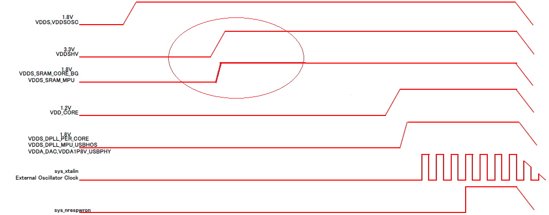
As per the current datasheet VDDS, VDDS_SRAM_CORE_BG/VDDS_SRAM_MPU/VDDSOSC
all are ramped together as shown below.


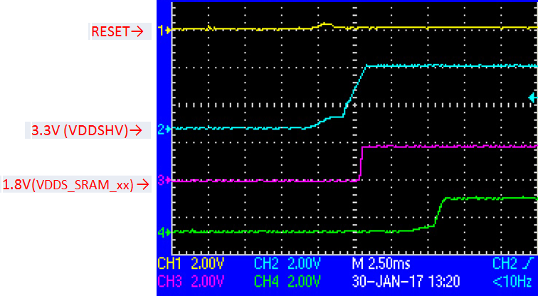
But in our customer's circuit,VDDS_SRAM_MPU/VDDS_SRAM_CORE_BG is ramped up
together or before VDDSHV(3.3V) as shown below.


And looking at the older datasheet, it says you can ramp up VDDS_SRAM_MPU/VDDS_SRAM_CORE_BG
after VDDSHV(3.3V).
So we believe VDDS_SRAM_MPU/VDDS_SRAM_CORE_BG could be ramped up before or after VDDSHV
or together with VDDSHV if we VDDS(1.8V) is powered up first.


Please let us know if this kind of usage is allowed.

Best Regards
Kummi

  • Hi,

    Information in the latest datasheet overrides all older datasheet revisions. Section 5.8.1 from the AM35x Datasheet Rev. F states:

    1. IO 1.8V supply (VDDS), Band-gap and LDO supplies (VDDS_SRAM_CORE_BG, VDDS_SRAM_MPU) and oscillator supply (VDDSOSC) should come up first to a stable state.
    2. IO 3.3V (VDDSHV) supply should be ramped up next to a stable state.
    3. Core (VDD_CORE) supply follows next to a stable state.
    4. All the PLL supplies (VDDS_DPLL_PER_CORE, VDDS_DPLL_MPU_USBHOST) and 1.8 V complex IO supplies (VDDA_DAC, VDDA1P8V_USBPHY) should be ramped up next to a stable state.
    5. Finally, 3.3 V complex IO (VDDA_3P3V_USBPHY) should be ramped up.
    6. sys_nrespwron must be held low at the time the power supplies are ramped up till the time the sys_32k and sys_xtalin clocks are stable.

    The datasheet requirements must be followed to ensure proper device functionality. Failure to do so may result in device reliability issues or cause permanent damage to the device.

  • Hi Biser,

    Thank you very much for the information.

    Actually this application is same as the one we discussed in the below
    E2E last year. And I am sorry to bring up the same topic again.
    e2e.ti.com/.../1910912

    We got the suggestion from the above E2E saying..

    "If VDDS is the first powered up, there is no issue in powering VDDS_SRAM_xxx, VDDSOSC later.
    As also noted in the App note, if there is a common 1.8V powering all these rails, you can also combine them".

    So from this comment we believe that once VDDS is powered up ramping up VDDS_SRAM_MPU/VDDS_SRAM_CORE_BG
    later (after VDDSHV or before VDDSHV) is fine.
    But one thing we are not sure if it is fine when both VDDS_SRAM_MPU/VDDS_SRAM_CORE_BG and VDDSHV
    ramp at the same time.

    We understand this question is out of the datasheet contents but your suggestions
    will be helpful in rectifying the necessary circuit in the customer's application.

    Best Regards
    Kummi
  • Sorry, I had forgotten that. Sivak is from the factory team, so his comments on the other thread are correct. Sorry about the confusion.
  • Hi Biser,

    Thank you for the confirmation.

    But, as mentioned above we need one confirmation if it is fine when both VDDS_SRAM_MPU/VDDS_SRAM_CORE_BG
    and VDDSHV(3.3V) ramp at the same time.

    In our customer's design VDDS_SRAM_MPU/VDDS_SRAM_CORE_BG(1.8V)
    and VDDSHV(3.3V) supply seems to be ramping up almost simultaneously as shown below.
    If this is permissible we can continue with the current design.


    Best Regards
    Kummi

  • I have asked the factory team to comment. They will respond here.
  • Can you provide the detailed power-up / power-down diagram along with the timings involved? It is not clear whether this an actual scope measurement or a possible power-up scenario. Also, ensure that the power-down sequence as also discussed earlier is followed.

    Regards, Siva

  • Hi Siva,

    Thank you very much for considering this request.
    Below is the power-up diagram with the timings.

    Actually VDDS_SRAM_MPU/VDDS_SRAM_CORE_BG(1.8V) was designed to ramp up after VDDSHV(3.3V),
    but due to the variation in the 1.8V power circuit the  VDDS_SRAM_xx supply ramps close(1ms - 6ms) to VDDSHV,
    almost ramping simultaneously.

    Below is the actual power-up timing screenshot from the oscilloscope.

    (Green CH4 is 1.8V(DPLL))


    Regarding the Power down sequence we got suggestions from you last year
    on a different E2E post and the difference between is 1.8V(VDDS)and VDDSHV(3.3V)
    is maintained <2V as shown below.

    Please let us know if VDDS_SRAM_xx and VDDSHV(3.3V) simultaneous ramp during power-up is allowed.

    Best Regards
    Kummi

  • Please let me know if there is any suggestions on this.
  • He is traveling and it may take a couple of days until he replies here...sorry.

  • Hi Siva,

    I am sorry to bother you,
    Please let me know if there is any suggestions on this.
  • Any updates on this?
  • Kummi, sorry for the delay...I am escalating this one...

  • Hi Rogerio,

    Thank you...any updates? it will be very helpful if you could provide the conclusion as early as possible.

  • Correct. You can split the 1.8V VDDS_SRAM_CORE_BG and VDDS_SRAM_MPU 1.8V rails to be ramped up after VDDSHV (3.3V).

    Regards, Siva

  • Hi Siva,

    Thank you very much for the reply.

    I am sorry but, do mean our power up sequence is correct??

    Which means VDDS_SRAM_MPU/VDDS_SRAM_CORE_BG(1.8V) and VDDSHV(3.3V)
    simultaneously(Below) ramping is fine?  If yes, we shall continue with the current design.


    Best Regards
    Kummi

  • Kummi

    The power sequence for VDDS_SRAM_CORE_BG [1.8V] and VDDS_SRAM_MPU [1.8V] ramping together with VDDSHV [3.3V] as shown in your scope plot looks fine to me. I assume you are ramping VDDS and VDDS_OSC ramping first after RESET is applied as per the requirement in the data sheet.

    It appears that VDDSHV supply ramp is not linear from your scope plot. Did you find out what is causing this behavior? It looks like the green waveform (not sure what supply this is) is also not linear.

    Regards, Siva

  • Hi Siva,

    Thank you very much for the help.
    We shall continue with the current design.

    Yes we are ramping VDDS and VDDS_OSC ramping first after
    RESET is applied as per the requirement in the data sheet.

    The non-linear behavior of VDDSHV supply is because of
    the soft start feature of the power supply which is used in order to
    match the power-up sequence of AM3505.

    Best Regards
    Kummi