


Hi,
I'm currently reading the Keystone Architecture DDR3 Memory Controller datasheet. I'm on the chapter about how the logical address is mapped to the DDR.
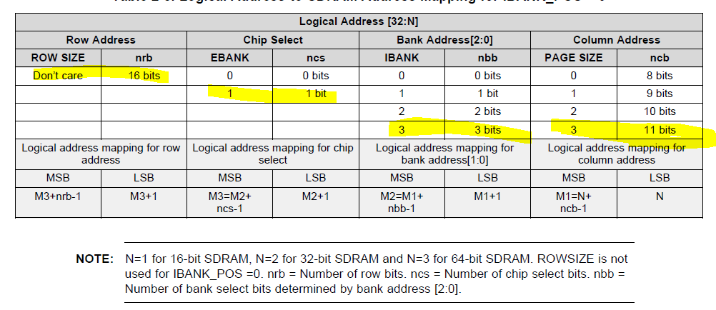
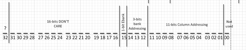
There is one sentence that got me confused. It is on page 22, "The DDR3 memory controller receives DDR3 memory access requests along with a 33-bit logical address from the rest of the system. The controller uses the logical address to generate a row/page, column, bank address, and chip selects for the DDR3 SDRAM"
I'm working with the CC6678 DSP and it has a 32 bit logical address. [31:0] So I'm confused what happens to the most significant bit [32:0] ?
Ex:
(I also took a look at the "DDR2 Memory Controller Datasheet" and it states 32-bit logical address)
Best,
Alvaro
