This thread has been locked.

If you have a related question, please click the "Ask a related question" button in the top right corner. The newly created question will be automatically linked to this question.

AISgen fails to configure DDR2

Other Parts Discussed in Thread: OMAPL138, TMS320C6748, OMAP-L138

Hi,


I have sample application which runs OK from either IRAM and DDR2 when using JTAG.

When I program the two versions (IRAM and DDR2) to a parallel NOR flash, the IRAM version runs OK, but the DDR2 fails.

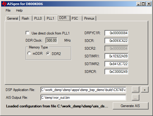
My conclusion is that the AISgen fails to initialize the DDR2.


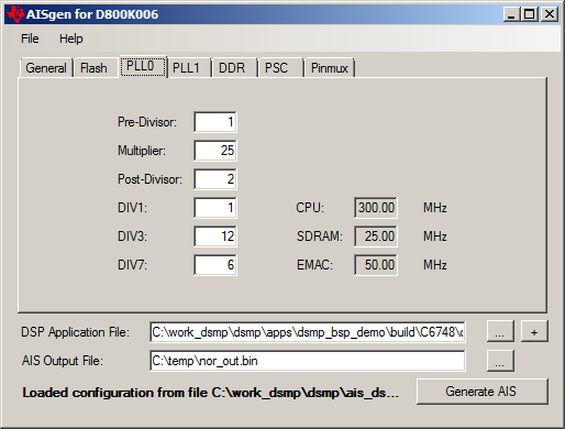
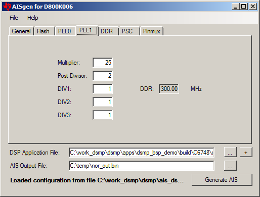
The C6748 runs at 300MHz, the DDR2 runs at 150MHz (top speed of the DSP's DDR controller).


Any idea what I did wrong?


Regards,

Uri


This is the GEL section for the DDR2 (known to work OK):


DEVICE_mDDRConfig(unsigned int freq) {
    int i;

   
    #define DRPYC1R                (DDRCTL)

    #define SDCR2_BOOTUNLOCK    (0x00800000)
    #define SDCR2_TIMUNLOCK        (0x00008000)

   
    GEL_TextOut("\tDEVICE_mDDRConfig %d MHz","Output",1,1,1, freq);
   
    /* 2.13.2    [1] */
    // Done @ device_PLL1()

    /* 2.13.2    [2] */
    // Enable the Clock to EMIF3A SDRAM/DDR
    PSC1_LPSC_enable(PD0, LPSC_DDR);
   
     /* 2.13.2    [3] */
    // VTP IO calibration
    #define VTP_CLKRZ            (0x00002000)
    #define VTP_LOCK            (0x00000080)
    #define VTP_POWERDN            (0x00000040)
    #define VTP_READY            (0x00008000)
    #define VTP_IOPWRDN            (0x00004000)
   
    VTPIO_CTL &= ~( VTP_CLKRZ | VTP_LOCK | VTP_POWERDN );    // a
    for (i = 0; i++; i<10) {}                                // a
    VTPIO_CTL |= VTP_CLKRZ;                                    // b
    while(!((VTPIO_CTL & VTP_READY) >> 15)) {}                // c
    VTPIO_CTL |= VTP_IOPWRDN;                                // d
    VTPIO_CTL |= VTP_LOCK;                                    // e
    VTPIO_CTL |= VTP_POWERDN;                                // f
   
    GEL_TextOut("\tVTP calibration completed","Output",1,1,1);
    /* 2.13.2    [4] */
    // DDR PHY control register 1
    DRPYC1R = 0x84; // EXT_STRBEN = External strobe. RL = (CAS latency + 1)
   
   
    /* 2.13.2    [7] */
   
        /* 2.13.1    [7 2] */
        // Program the SDRAM configuration register (SDCR) with BOOTUNLOCK bit set to 1 (unlocked).
        EMIF3A_SDCR |= SDCR2_BOOTUNLOCK;
        EMIF3A_SDCR |= SDCR2_TIMUNLOCK;
       
        /* 2.13.1    [7 3] */
        EMIF3A_SDCR = 0x0093C622; // BOOTUNLOCK locked
        EMIF3A_SDCR &= ~(SDCR2_BOOTUNLOCK); // BOOTUNLOCK locked
       
        /* 2.13.1    [7 4] */
        // SDCR2
        EMIF3A_SDCR2   = 0x00000004; // 8K rows  

        /* 2.13.1    [7 5] */
        // Timers
        EMIF3A_SDTIMR1 = 0x1E922A09;
        EMIF3A_SDTIMR2 = 0x8412C722;
       
        /* 2.13.1    [7 6] */
        // TIMUNLOCK locked
        EMIF3A_SDCR &= ~(SDCR2_TIMUNLOCK);
       
        /* 2.13.1    [7 7] */
        // Refresh rate
        EMIF3A_SDRCR = 0x00000249 | (0x1 << 30) | (0x1 << 31); /* The two MSB bits are per correction from the forum */
       
    /* 2.13.2    [5] */
    // PSC reset
    PSC1_LPSC_SyncReset(PD0, LPSC_DDR);
    PSC1_LPSC_enable(PD0, LPSC_DDR);

    /* 2.13.2    [6] */
    // 00h will ensure master priority is strictly honored (at the cost of decreased
    // DDR2/mDDR memory controller efficiency)
    EMIF3A_PBBPR = 0x20;

}


The AISgen configuration is:


  • Check the DDR configuration registers at 0xB0000000 after you boot from NOR. Run the GEL file and see if any values change.

    After you boot from NOR are you able to successfully modify the memory contents? Open up the memory window at 0xC0000000 and try to read and write. If it fails, use the gel and try to determine what it is doing differently.

    Jeff

  • some observations:

    1)  There is debug (CCS4/JTAG emulator) R/W access to the DDR2 after boot from the parallel flash ( [!!] note that a while ago it was seemed that I have access to the DDR2 when booting using CCS4/JTAG emulator with GEL, but it failed to run a program properly, later on, after multiple discussion with TI support and in this forum, it has been discovered that there are errors in the DDR2 documentation (sprugj4.pdf) and there is different initialization sequence which should be applied in order the DDR2 to work correctly. (http://e2e.ti.com/support/dsp/tms320c6000_high_performance_dsps/f/115/p/53004/188117.aspx#188117), only after modifying the GEL sequence the DDR2 initialization has been done successfully)

    Maybe we have the same problem with the AISgen?


    2) The value at address 0xB0000014 (Timer 2) is different from the value I set in the AISgem (0x8412C722 and 0x0412C722 correspondingly)

    3) The value of SDRCR is different too (Read value from register: 0x00000249, originally set value: 0xC0000249)


    Regards,

    Uri

  • Hi Uri

    I don't think the issue with the sequence should be impacting the AISGEN tool ( I am saying this with a bit of uncertainty because I don't have a DDR2 based board to test this out). However it does seem to work fine on the Hawkboard , as documented http://elinux.org/Hawkboard

    Which is also an OMAPL138/C6748 family board but with DDR2 on it.

    When you had the issue with the sequence, I recall that you were experiencing a hang,  I don't believe you are seeing a hang when executing from NOR flash to initialize DDR2 via AIS configuration (Please correct me if I am wrong).


    Uri Shkolnik said:
    2) The value at address 0xB0000014 (Timer 2) is different from the value I set in the AISgem (0x8412C722 and 0x0412C722 correspondingly)

    I believe this should be a don't care SDTIMR2 bit 31 is reserved as per the documentation, so you should see a 0x0412C722 even though you tried to write a 1 to bit 31?[

    Uri Shkolnik said:
    The value of SDRCR is different too (Read value from register: 0x00000249, originally set value: 0xC0000249)

    Can you try a value of 0x249 , and see if that works?

    Can you clarify on Jeff's query on what happens when you try to access the DDR2 memory space after the NOR flash execution? You can also compare whether or not you see the expected code getting loaded into DDR2 region, comparing the memory content with the scenario you have working well using CCSv4+ GEL file etc.

    It will also help if you could share your AISCFG file for the DDR2 configuration (the one you have snapshotted in this post). Please also confirm what is the ROMID for the device you are using.

    Regards

    Mukul


  • Also even though I think it should be a don't care, please see if not enabling DDR2 via PSC in the config file explicitly helps. Since you are using AISGEN to configure the DDR2, I don't think you need to have that additionally done in the PSC tab.

    Regards

    Mukul

  • Mukul, Jeff and all,


    Steps I have taken -

    1) Remove PSC #6 (DDR) from the PSC tab - no change

    2) Change the SDRCRto 0x249 - no change


    The ROMID is "d800k004" (re-checked)

    The AISgen configuration file is attached inline below.


    Regards,

    Uri


    Boot Mode=NOR Flash
    Boot Speed=0
    Flash Width=1
    Flash Timing=3ffffffd
    Configure Peripheral=False
    Configure PLL0=True
    Configure SDRAM=False
    Configure PLL1=True
    Configure DDR2=True
    Configure LPSC=True
    Configure Pinmux=True
    Enable CRC=False
    Specify Entrypoint=False
    Enable Sequential Read=False
    Use 4.5 Clock Divider=False
    Use DDR2 Direct Clock=False
    Use mDDR=False
    ROM ID=1
    Device Type=1
    Input Clock Speed=24
    Clock Type=0
    PLL0 Pre Divider=1
    PLL0 Multiplier=25
    PLL0 Post Divider=2
    PLL0 Div1=1
    PLL0 Div3=12
    PLL0 Div7=6
    PLL1 Multiplier=25
    PLL1 Post Divider=2
    PLL1 Div1=1
    PLL1 Div2=2
    PLL1 Div3=3
    Entrypoint=0
    SDRAM SDBCR=0
    SDRAM SDTMR=0
    SDRAM SDRSRPDEXIT=0
    SDRAM SDRCR=0
    DDR2 PHY=84
    DDR2 SDCR=93c622
    DDR2 SDCR2=4
    DDR2 SDTIMR=1e922a09
    DDR2 SDTIMR2=8412c722
    DDR2 SDRCR=249
    LPSC0 Enable=0+1+2+3+4+9+10+11+12+13+15+
    LPSC0 Disable=5+
    LPSC0 SyncRst=
    LPSC1 Enable=0+1+3+10+11+12+13+19+21+24+25+26+27+28+29+30+31+
    LPSC1 Disable=2+4+5+7+8+9+14+15+16+17+18+20+
    LPSC1 SyncRst=
    Pinmux=0:88888888+1:88888888+2:44444448+3:44221101+4:22222214+5:81108111+6:88888888+7:88111111+8:11111111+9:11111111+10:11111111+11:11111111+12:11111111+13:44448888+14:44444480+15:44444444+16:44444444+17:44444444+18:88444444+19:88888888+
    App File String=C:\work_dsmp\dsmp\apps\led_flash_test\build\C6748\ccs4\Debug\systest.out
    AIS File Name=C:\work_dsmp\bin2source\bin2source\Debug\led_ddr2_UART2.bin

  • Uri

    Thanks for sharing the cfg file, I can't see anything visibly wrong here. I have not cross-verified your DDR register settings, I assume those are more or less working for you for your board, when you program the same value using the GEL file.

    Can you please clarify , what you mean by your "application fails", what are the failure symptoms.

    Since you say that it works if you put everything in IRAM, for completeness can you also post your cfg file when using IRAM.

    Regards

    Mukul

  • Mukul,


    The application is very simple, it causes a LED (GPIO as O) to blink. (wow :-))

    I built the application twice: [1] Linked to IRAM (only) [2] Linked to DDR2

    When using JTAG + GEL, both [1] & [2] run, aka, the LED blinks.

    When booting from parallel NOR flash (using the AISgen as image generator), [1] runs (LED blinks), and [2] fails (no LED activity)

    The CFG file for both [1] & [2] is the same. (The linker directives, during build, are different, that's all)


    Regards,

    Uri

  • Hi Uri

    I tried the LED blink test ( that comes with LogicPD BSL) with the EVM ( has mDDR) and it seems to work fine (placing all the code in mDDR instead of Shared RAM etc). The cfg file looks more or less identical (except for differences in the DDR configuration register settings). Still not able to pin point what might be going wrong in your setup

    Can you also confirm that you are not doing any DDR2 and PINMUX initialization in your application code? If you are using the AISGEN for this, you would not need to have any DDR2/pinmux etc done via the application code. If you do any SYSCFG register configuration in your application code (like PINMUX reg or VTP control etc) you would  need to ensure that ARM is in supervisor mode.

    Regards

    Mukul

  • You can ignore my question, I see from your post that linking to IRAM vs DDR2 is the only change in your application

    Uri Shkolnik said:
    I built the application twice: [1] Linked to IRAM (only) [2] Linked to DDR2

  • ok.


    Regarding "ARM is in supervisor mode", please note I'm using C6748 only. (no OMAP)


    Uri

  • Uri

    Thanks for the additional clarification, I did loose track that I am helping debug the c6748 not the OMAPL138.

    I have managed to find a DDR2 based board, and tried to run several experiments using the AISGEN running a led blink type program from internal and external memory, and I am not able to see any issues.

    At this point , I would suspect that something may not be right with your custom board DDR2 or setup.

    I had some additional quesitons

    1) Are you sure that the DDR2 works reliably. Do you have some simple read/write test that pass reliably at 150 MHz on your board?

    2) Should I assume that your LED blink test running from external memory always passes reliably?

    3) What tools/utilities are you using to flash the NOR flash? If you are using the serial boot utilities , are you keeping in considerations the guidelines for custom boards , toward the end of the wiki ( http://processors.wiki.ti.com/index.php/Serial_Boot_and_Flash_Loading_Utility_for_OMAP-L138)

    4) When your application running from DDR2 does not result in LED Blink, can you connect to CCS and tell us the program counter location?

    Regards

    Mukul


  • Mukul,


    [1] The custom board runs an application which contains USB stack, uPP stack, 3xUART (one is muxed to two peripherals) , I2C (several peripherals), 2x SPI (multiple peripherals), and quite large application. Everything is linked to the DDR (IRAM is kept for specific algorithms), everything runs (using JTAG + GEL) smoothly,

    The DDR clock has been checked, using 500MHz oscillator, and it is verified to work at 150MHz.

    [2] Yes, while using JTAG + GEL

    [3] I'm using driver from the manufacture for chip_erase() and program_buffer(). I compare the flash content (after programming) with the file contains the AISgen output, they are identical, The AISgen is configured for NOR flash (CS2), 16-bit, maximum wait-states.

    [4] I'll check it tomorrow, I'm away from my lab today.


    Regards,

    Uri


  • Hi,


    Please find below the PC, and various other core registers

    It seems that multiple elements failed to be configured (DDR2, Pinmux, etc), when the application is configured to boot from DDR2.


    4135.c6748_regs.zip


    Regards,

    Uri


  • Hi Uri

    Thanks for sending the register dump.I quickly conferred with the boot loader experts, and the first thing we notice is that the bootmode seem to be UART1 boot not NOR boot.  This seems to be what is being indicated by the program counter also, it seems to be stuck in the UART boot waiting to receive a byte.

    Is this expected behavior?

    BTW, the amount of information that is in the register dump is impressive. How did you manage to collect so much data (I hope it was not a manual process).

    Regards

    Mukul

  • By the way, the GEL file here: http://processors.wiki.ti.com/index.php/OMAP-L1x_Debug_Gel_Files might help you verify your bootmode and check for any rom error messages.

    Jeff

  • Hi Mulul,

    It's my mistake (the UART mode), I tried something with UART and forgot about it when I have recorded the registers status.

    Anyway, I re-sent the registers capture.

    The output of the GEL file (http://processors.wiki.ti.com/index.php/File:OMAPL1x_debug.zip):


    C674X_0: Output: ---------------------------------------------
    C674X_0: Output: |               BOOTROM Info                |
    C674X_0: Output: ---------------------------------------------
    C674X_0: Output: ROM ID: d800k004 
    C674X_0: Output: Silicon Revision 1.1
    C674X_0: Output: Boot Mode: NOR
    C674X_0: Output:  ROM Status Code: 0x00000000  Description:
    C674X_0: Output: No error


    The registers are captured using:

    1) CCS4 --> Debug perspective --> (Tools) View --> Registers

    2) Right-click on empty space in the Registers windows, and select 'save all registers'

    and the output is below.


    Regards,


    Uri


    Core Registers
        PC = 0x00713DA0
        CLK = 0x00000000
        SP = 0x00F00688
        FP = 0x00F00688
        A0 = 0x001861B7
        A1 = 0x00000000
        A2 = 0x00000018
        A3 = 0x007121F0
        A4 = 0x01E2C000
        A5 = 0x00F00014
        A6 = 0x00000000
        A7 = 0x11810D80
        A8 = 0x00000249
        A9 = 0x118115B4
        A10 = 0x00000000
        A11 = 0x00000000
        A12 = 0x00000000
        A13 = 0x00000000
        A14 = 0x00000000
        A15 = 0x00000000
        A16 = 0xC002AAE8
        A17 = 0x00000000
        A18 = 0x000000A8
        A19 = 0x23B45A02
        A20 = 0x1554F553
        A21 = 0x45732CE7
        A22 = 0x567DDA84
        A23 = 0x3B72DAE1
        A24 = 0x00000000
        A25 = 0x43D5F133
        A26 = 0xA4B673C9
        A27 = 0xAB9FD859
        A28 = 0x47632884
        A29 = 0x9F3FF67D
        A30 = 0x1180DF90
        A31 = 0x118111A0
        B0 = 0x0018C1B7
        B1 = 0x00000003
        B2 = 0x00000000
        B3 = 0x00713D64
        B4 = 0x01E2C000
        B5 = 0x00713784
        B6 = 0x00000003
        B7 = 0x00713D18
        B8 = 0x00000000
        B9 = 0xC001B490
        B10 = 0x00000084
        B11 = 0x00000000
        B12 = 0x00000000
        B13 = 0x00000000
        B14 = 0xC002CF40
        B15 = 0x00F00688
        B16 = 0x00000010
        B17 = 0xC0024EC8
        B18 = 0x0A22A50E
        B19 = 0x0A22A50E
        B20 = 0x6B1B211C
        B21 = 0xAF6BE142
        B22 = 0x4008218E
        B23 = 0xF2FF25A9
        B24 = 0x00000000
        B25 = 0x2A5BCA65
        B26 = 0x88B22171
        B27 = 0x372BDED8
        B28 = 0xB4AEFA4A
        B29 = 0x9A69F014
        B30 = 0x01E26000
        B31 = 0x00000002
        AMR = 0x00000000
            _RESV = 0x0
            BK1 = 0x0
            BK0 = 0x0
            B7MODE = LINEAR (0x0)
            B6MODE = LINEAR (0x0)
            B5MODE = LINEAR (0x0)
            B4MODE = LINEAR (0x0)
            A7MODE = LINEAR (0x0)
            A6MODE = LINEAR (0x0)
            A5MODE = LINEAR (0x0)
            A4MODE = LINEAR (0x0)
        CSR = 0x14000100
            CPU_ID = 0x14
            REV_ID = 0x0
            PWRD = 0x0
            SAT = NONSATURATE (0x0)
            EN = LITTLE (0x1)
            PCC = 0x0
            DCC = 0x0
            PGIE = 0x0
            GIE = DISABLE (0x0)
        IFR = 0x00000000
            _RESV = ****************
            IF15 = 0x0
            IF14 = 0x0
            IF13 = 0x0
            IF12 = 0x0
            IF11 = 0x0
            IF10 = 0x0
            IF9 = 0x0
            IF8 = 0x0
            IF7 = 0x0
            IF6 = 0x0
            IF5 = 0x0
            IF4 = 0x0
            _RESV = **
            NMIF = 0x0
            _RESV = *
        ISR = 0x00000000
            _RESV = 0x0
            IS15 = 0x0
            IS14 = 0x0
            IS13 = 0x0
            IS12 = 0x0
            IS11 = 0x0
            IS10 = 0x0
            IS9 = 0x0
            IS8 = 0x0
            IS7 = 0x0
            IS6 = 0x0
            IS5 = 0x0
            IS4 = 0x0
            _RESV = ****
        ICR = 0x00000000
            _RESV = 0x0
            IC15 = 0x0
            IC14 = 0x0
            IC13 = 0x0
            IC12 = 0x0
            IC11 = 0x0
            IC10 = 0x0
            IC9 = 0x0
            IC8 = 0x0
            IC7 = 0x0
            IC6 = 0x0
            IC5 = 0x0
            IC4 = 0x0
            _RESV = ****
        IER = 0x00000001
            _RESV = ****************
            IE15 = DISABLE (0x0)
            IE14 = DISABLE (0x0)
            IE13 = DISABLE (0x0)
            IE12 = DISABLE (0x0)
            IE11 = DISABLE (0x0)
            IE10 = DISABLE (0x0)
            IE09 = DISABLE (0x0)
            IE08 = DISABLE (0x0)
            IE07 = DISABLE (0x0)
            IE06 = DISABLE (0x0)
            IE05 = DISABLE (0x0)
            IE04 = DISABLE (0x0)
            _RESV = **
            NMI = 0x0
            Reserved = *
        ISTP = 0x00700000
            ISTB = 0x1c00
            HPEINT = 0x0
            _RESV = 0x0
        IRP = 0x00000000
        NRP = 0x00000000
        ERP = 0x00000000
        TSCL = 0x00000000
        TSCH = 0x00000000
        ARP = 0x00000000
        ILC = 0x00000000
        RILC = 0x00000000
        PCE1 = 0x00713DA0
        DNUM = 0x00000001
            _RESV = 0x0
            DSPNUM = 0x1
        FADCR = 0x00000000
        FAUCR = 0x00000000
        FMCR = 0x00000000
        SSR = 0x00000000
            RESV = 0x0
            M2 = 0x0
            M1 = 0x0
            S2 = 0x0
            S1 = 0x0
            L2 = 0x0
            L1 = 0x0
        GPLYA = 0x00000000
        GPLYB = 0x00000000
        GFPGFR = 0x0700001D
            _RESV = 0x0
            SIZE = 0x7
            _RESV = 0x0
            POLY = 0x1d
        DIER = 0x00000000
        TSR = 0x00000000
            _RESV = 0x0
            IB = UNBLOCKED (0x0)
            SPLX = NOTEXEC (0x0)
            _RESV = 0x0
            EXC = NOTEXEC (0x0)
            INT = NOTEXEC (0x0)
            _RESV = 0x0
            CXM = SUPERVISOR (0x0)
            _RESV = 0x0
            DBGM = EMU_ENABLE (0x0)
            XEN = DISABLE (0x0)
            GEE = DISABLE (0x0)
            SGIE = 0x0
            GIE = DISABLE (0x0)
        ITSR = 0x00000000
            _RESV = 0x0
            IB = UNBLOCKED (0x0)
            SPLX = NOTEXEC (0x0)
            _RESV = 0x0
            EXC = NOTEXEC (0x0)
            INT = NOTEXEC (0x0)
            _RESV = 0x0
            CXM = SUPERVISOR (0x0)
            _RESV = 0x0
            DBGM = EMU_ENABLE (0x0)
            XEN = DISABLE (0x0)
            GEE = DISABLE (0x0)
            SGIE = 0x0
            GIE = DISABLE (0x0)
        NTSR = 0x00000000
            _RESV = 0x0
            IB = UNBLOCKED (0x0)
            SPLX = NOTEXEC (0x0)
            _RESV = 0x0
            EXC = NOTEXEC (0x0)
            INT = NOTEXEC (0x0)
            _RESV = 0x0
            CXM = SUPERVISOR (0x0)
            _RESV = 0x0
            DBGM = EMU_ENABLE (0x0)
            XEN = DISABLE (0x0)
            GEE = DISABLE (0x0)
            SGIE = 0x0
            GIE = DISABLE (0x0)
        ETSR = 0x00000000
            _RESV = 0x0
            IB = 0x0
            SPLX = 0x0
            _RESV = 0x0
            EXC = 0x0
            INT = 0x0
            _RESV = 0x0
            CXM = 0x0
            _RESV = 0x0
            DBGM = 0x0
            XEN = 0x0
            GEE = 0x0
            SGIE = 0x0
            GIE = 0x0
        EFR = 0x00000000
            NXF = 0x0
            EXF = 0x0
            _RESV = 0x0
            IXF = 0x0
            OXF = 0x0
        ECR = 0x00000000
            NXC = 0x0
            EXC = 0x0
            _RESV = 0x0
            IXC = 0x0
            OXC = 0x0
        IERR = 0x00000000
    RegisterPairs
        A1_A0 = 0x00000000001861B7
        A3_A2 = 0x007121F000000018
        A5_A4 = 0x00F0001401E2C000
        A7_A6 = 0x11810D8000000000
        A9_A8 = 0x118115B400000249
        A11_A10 = 0x0000000000000000
        A13_A12 = 0x0000000000000000
        A15_A14 = 0x0000000000000000
        A17_A16 = 0x00000000C002AAE8
        A19_A18 = 0x23B45A02000000A8
        A21_A20 = 0x45732CE71554F553
        A23_A22 = 0x3B72DAE1567DDA84
        A25_A24 = 0x43D5F13300000000
        A27_A26 = 0xAB9FD859A4B673C9
        A29_A28 = 0x9F3FF67D47632884
        A31_A30 = 0x118111A01180DF90
        B1_B0 = 0x000000030018C1B7
        B3_B2 = 0x00713D6400000000
        B5_B4 = 0x0071378401E2C000
        B7_B6 = 0x00713D1800000003
        B9_B8 = 0xC001B49000000000
        B11_B10 = 0x0000000000000084
        B13_B12 = 0x0000000000000000
        B15_B14 = 0x00F00688C002CF40
        B17_B16 = 0xC0024EC800000010
        B19_B18 = 0x0A22A50E0A22A50E
        B21_B20 = 0xAF6BE1426B1B211C
        B23_B22 = 0xF2FF25A94008218E
        B25_B24 = 0x2A5BCA6500000000
        B27_B26 = 0x372BDED888B22171
        B29_B28 = 0x9A69F014B4AEFA4A
        B31_B30 = 0x0000000201E26000
    SYSCFG0DSP
        REVID = 0x4E840102
            REVID = 0x4e840102
        DIEIDR0 = 0x0300D022
            DIEID0 = 0x300d022
        DIEIDR1 = 0x0061E59F
            DIEID1 = 0x61e59f
        DIEIDR2 = 0x00000000
            DIEID2 = 0x0
        DIEIDR3 = 0x62AE0001
            DIEID3 = 0x62ae0001
        DEVIDR0 = 0x0B7D102F
            DEVID0 = 0xb7d102f
        BOOTCFG = 0x00000002
            _RESV_1 = ****
            SMARTRFLX = 0x0
            BOOTMODE = 0x2
        CHIPREVIDR = 0x00000001
            _RESV_1 = **************************
            CHIPREVID = 0x1
        KICK0R = 0x00000000
            KICK0 = 0x0
        KICK1R = 0x00000000
            KICK1 = 0x0
        HOST0CFG = 0x00000000
            BOOTRDY = 0x0
            _RESV_2 = *******************************
        HOST1CFG = 0x00700001
            BOOTRDY = 0x0
            _RESV_2 = *********
            DSP_ISTP_RST_VAL = 0x300001
        IRAWSTAT = 0x00000000
            _RESV_1 = ******************************
            ADDRERR = NOTSET (0x0)
            PROTERR = NOTSET (0x0)
        IENSTAT = 0x00000000
            _RESV_1 = ******************************
            ADDRERR = NOTSET (0x0)
            PROTERR = NOTSET (0x0)
        IENSET = 0x00000000
            _RESV_1 = ******************************
            ADDRERR_EN =
            PROTERR_EN =
        IENCLR = 0x00000000
            _RESV_1 = ******************************
            ADDRERR_CLR =
            PROTERR_CLR =
        EOI = 0x00000000
            _RESV_1 = ************************
            EOIVECT = ********
        FLTADDRR = 0x00000000
            FLTADDR = 0x0
        FLTSTAT = 0x00000000
            ID = 0x0
            MSTID = 0x0
            _RESV_3 = ***
            PRIVID = 0x0
            _RESV_5 = *
            NOSECACC = 0x0
            _RESV_7 = *
            TYPE = NOFLT (0x0)
        MSTPRI0 = 0x44442222
            _RESV_1 = *********
            SATA = 0x4
            _RESV_3 = *
            UPP = 0x4
            _RESV_5 = *
            DSP_CFG = 0x2
            _RESV_7 = *
            DSP_MDMA = 0x2
            _RESV_9 = *
            ARM_D = 0x2
            _RESV_11 = *
            ARM_I = 0x2
        MSTPRI1 = 0x44440000
            _RESV_1 = *
            VPIF_DMA_1 = 0x4
            _RESV_3 = *
            VPIF_DMA_0 = 0x4
            _RESV_5 = *****
            EDMA31TC0 = 0x4
            _RESV_7 = *
            EDMA30TC1 = 0x0
            _RESV_9 = *
            EDMA30TC0 = 0x0
            _RESV_11 = *
            _RESV_12 = ***
            _RESV_13 = *
            _RESV_14 = ***
        MSTPRI2 = 0x54604404
            _RESV_1 = *
            LCDC = 0x5
            _RESV_3 = *
            USB1 = 0x4
            _RESV_5 = *
            UHPI = 0x6
            _RESV_7 = *****
            USB0CDMA = 0x4
            _RESV_9 = *
            USB0CFG = 0x4
            _RESV_11 = *****
            EMAC = 0x4
        PINMUX0 = 0x88888888
            PINMUX0_31_28 = GPIO0_8 (0x8)
            PINMUX0_27_24 = GPIO0_9 (0x8)
            PINMUX0_23_20 = GPIO0_10 (0x8)
            PINMUX0_19_16 = GPIO0_11 (0x8)
            PINMUX0_15_12 = GPIO0_12 (0x8)
            PINMUX0_11_8 = GPIO0_13 (0x8)
            PINMUX0_7_4 = GPIO0_14 (0x8)
            PINMUX0_3_0 = GPIO0_15 (0x8)
        PINMUX1 = 0x88888888
            PINMUX1_31_28 = GPIO0_0 (0x8)
            PINMUX1_27_24 = GPIO0_1 (0x8)
            PINMUX1_23_20 = GPIO0_2 (0x8)
            PINMUX1_19_16 = GPIO0_3 (0x8)
            PINMUX1_15_12 = GPIO0_4 (0x8)
            PINMUX1_11_8 = GPIO0_5 (0x8)
            PINMUX1_7_4 = GPIO0_6 (0x8)
            PINMUX1_3_0 = GPIO0_7 (0x8)
        PINMUX2 = 0x44444448
            PINMUX2_31_28 = GPIO8_7 (0x4)
            PINMUX2_27_24 = GPIO1_9 (0x4)
            PINMUX2_23_20 = GPIO1_10 (0x4)
            PINMUX2_19_16 = GPIO1_11 (0x4)
            PINMUX2_15_12 = GPIO1_12 (0x4)
            PINMUX2_11_8 = GPIO1_13 (0x4)
            PINMUX2_7_4 = GPIO1_14 (0x4)
            PINMUX2_3_0 = GPIO1_15 (0x8)
        PINMUX3 = 0x44221101
            PINMUX3_31_28 = GPIO8_1 (0x4)
            PINMUX3_27_24 = GPIO8_2 (0x4)
            PINMUX3_23_20 = UART0_TXD (0x2)
            PINMUX3_19_16 = UART0_RXD (0x2)
            PINMUX3_15_12 = SPI0_SIMO0 (0x1)
            PINMUX3_11_8 = SPI0_SOMI0 (0x1)
            PINMUX3_7_4 = Default (0x0)
            PINMUX3_3_0 = SPI0_CLK (0x1)
        PINMUX4 = 0x22222214
            PINMUX4_31_28 = UART1_TXD (0x2)
            PINMUX4_27_24 = UART1_RXD (0x2)
            PINMUX4_23_20 = UART2_TXD (0x2)
            PINMUX4_19_16 = UART2_RXD (0x2)
            PINMUX4_15_12 = I2C0_SDA (0x2)
            PINMUX4_11_8 = I2C0_SCL (0x2)
            PINMUX4_7_4 = nSPI0_SCS0 (0x1)
            PINMUX4_3_0 = GPIO1_7 (0x4)
        PINMUX5 = 0x11108111
            PINMUX5_31_28 = EMA_BA0 (0x1)
            PINMUX5_27_24 = EMA_BA1 (0x1)
            PINMUX5_23_20 = SPI1_SIMO0 (0x1)
            PINMUX5_19_16 = Default (0x0)
            PINMUX5_15_12 = GPIO2_12 (0x8)
            PINMUX5_11_8 = SPI1_CLK (0x1)
            PINMUX5_7_4 = nSPI1_SCS0 (0x1)
            PINMUX5_3_0 = nSPI1_SCS1 (0x1)
        PINMUX6 = 0x88888888
            PINMUX6_31_28 = GPIO2_0 (0x8)
            PINMUX6_27_24 = GPIO2_1 (0x8)
            PINMUX6_23_20 = GPIO2_2 (0x8)
            PINMUX6_19_16 = GPIO2_3 (0x8)
            PINMUX6_15_12 = GPIO2_4 (0x8)
            PINMUX6_11_8 = GPIO2_5 (0x8)
            PINMUX6_7_4 = GPIO2_6 (0x8)
            PINMUX6_3_0 = GPIO2_7 (0x8)
        PINMUX7 = 0x88111111
            PINMUX7_31_28 = GPIO3_8 (0x8)
            PINMUX7_27_24 = GPIO3_9 (0x8)
            PINMUX7_23_20 = nEMA_OE (0x1)
            PINMUX7_19_16 = nEMA_WE (0x1)
            PINMUX7_15_12 = nEMA_CS5 (0x1)
            PINMUX7_11_8 = nEMA_CS4 (0x1)
            PINMUX7_7_4 = nEMA_CS3 (0x1)
            PINMUX7_3_0 = nEMA_CS2 (0x1)
        PINMUX8 = 0x11111111
            PINMUX8_31_28 = EMA_D8 (0x1)
            PINMUX8_27_24 = EMA_D9 (0x1)
            PINMUX8_23_20 = EMA_D10 (0x1)
            PINMUX8_19_16 = EMA_D11 (0x1)
            PINMUX8_15_12 = EMA_D12 (0x1)
            PINMUX8_11_8 = EMA_D13 (0x1)
            PINMUX8_7_4 = EMA_D14 (0x1)
            PINMUX8_3_0 = EMA_D15 (0x1)
        PINMUX9 = 0x11111111
            PINMUX9_31_28 = EMA_D0 (0x1)
            PINMUX9_27_24 = EMA_D1 (0x1)
            PINMUX9_23_20 = EMA_D2 (0x1)
            PINMUX9_19_16 = EMA_D3 (0x1)
            PINMUX9_15_12 = EMA_D4 (0x1)
            PINMUX9_11_8 = EMA_D5 (0x1)
            PINMUX9_7_4 = EMA_D6 (0x1)
            PINMUX9_3_0 = EMA_D7 (0x1)
        PINMUX10 = 0x11111111
            PINMUX10_31_28 = EMA_A16 (0x1)
            PINMUX10_27_24 = EMA_A17 (0x1)
            PINMUX10_23_20 = EMA_A18 (0x1)
            PINMUX10_19_16 = EMA_A19 (0x1)
            PINMUX10_15_12 = EMA_A20 (0x1)
            PINMUX10_11_8 = EMA_A21 (0x1)
            PINMUX10_7_4 = EMA_A22 (0x1)
            PINMUX10_3_0 = EMA_A23 (0x1)
        PINMUX11 = 0x11111111
            PINMUX11_31_28 = EMA_A8 (0x1)
            PINMUX11_27_24 = EMA_A9 (0x1)
            PINMUX11_23_20 = EMA_A10 (0x1)
            PINMUX11_19_16 = EMA_A11 (0x1)
            PINMUX11_15_12 = EMA_A12 (0x1)
            PINMUX11_11_8 = EMA_A13 (0x1)
            PINMUX11_7_4 = EMA_A14 (0x1)
            PINMUX11_3_0 = EMA_A15 (0x1)
        PINMUX12 = 0x11111111
            PINMUX12_31_28 = EMA_A0 (0x1)
            PINMUX12_27_24 = EMA_A1 (0x1)
            PINMUX12_23_20 = EMA_A2 (0x1)
            PINMUX12_19_16 = EMA_A3 (0x1)
            PINMUX12_15_12 = EMA_A4 (0x1)
            PINMUX12_11_8 = EMA_A5 (0x1)
            PINMUX12_7_4 = EMA_A6 (0x1)
            PINMUX12_3_0 = EMA_A7 (0x1)
        PINMUX13 = 0x44448888
            PINMUX13_31_28 = CH1_WAIT (0x4)
            PINMUX13_27_24 = CH1_ENABLE (0x4)
            PINMUX13_23_20 = CH1_START (0x4)
            PINMUX13_19_16 = CH1_CLK (0x4)
            PINMUX13_15_12 = GPIO6_12 (0x8)
            PINMUX13_11_8 = GPIO6_13 (0x8)
            PINMUX13_7_4 = GPIO6_14 (0x8)
            PINMUX13_3_0 = GPIO6_15 (0x8)
        PINMUX14 = 0x44444480
            PINMUX14_31_28 = UPP_D10 (0x4)
            PINMUX14_27_24 = UPP_D11 (0x4)
            PINMUX14_23_20 = UPP_D12 (0x4)
            PINMUX14_19_16 = UPP_D13 (0x4)
            PINMUX14_15_12 = UPP_D14 (0x4)
            PINMUX14_11_8 = UPP_D15 (0x4)
            PINMUX14_7_4 = GPIO6_6 (0x8)
            PINMUX14_3_0 = Default (0x0)
        PINMUX15 = 0x44444444
            PINMUX15_31_28 = UPP_D2 (0x4)
            PINMUX15_27_24 = UPP_D3 (0x4)
            PINMUX15_23_20 = UPP_D4 (0x4)
            PINMUX15_19_16 = UPP_D5 (0x4)
            PINMUX15_15_12 = UPP_D6 (0x4)
            PINMUX15_11_8 = UPP_D7 (0x4)
            PINMUX15_7_4 = UPP_D8 (0x4)
            PINMUX15_3_0 = UPP_D9 (0x4)
        PINMUX16 = 0x44444444
            PINMUX16_31_28 = UPP_XD10 (0x4)
            PINMUX16_27_24 = UPP_XD11 (0x4)
            PINMUX16_23_20 = UPP_XD12 (0x4)
            PINMUX16_19_16 = UPP_XD13 (0x4)
            PINMUX16_15_12 = UPP_XD14 (0x4)
            PINMUX16_11_8 = UPP_XD15 (0x4)
            PINMUX16_7_4 = UPP_D0 (0x4)
            PINMUX16_3_0 = UPP_D1 (0x4)
        PINMUX17 = 0x44444444
            PINMUX17_31_28 = UPP_XD2 (0x4)
            PINMUX17_27_24 = UPP_XD3 (0x4)
            PINMUX17_23_20 = UPP_XD4 (0x4)
            PINMUX17_19_16 = UPP_XD5 (0x4)
            PINMUX17_15_12 = UPP_XD6 (0x4)
            PINMUX17_11_8 = UPP_XD7 (0x4)
            PINMUX17_7_4 = UPP_XD8 (0x4)
            PINMUX17_3_0 = UPP_XD9 (0x4)
        PINMUX18 = 0x88444444
            PINMUX18_31_28 = GPIO8_10 (0x8)
            PINMUX18_27_24 = GPIO8_11 (0x8)
            PINMUX18_23_20 = CH0_WAIT (0x4)
            PINMUX18_19_16 = CH0_ENABLE (0x4)
            PINMUX18_15_12 = CH0_START (0x4)
            PINMUX18_11_8 = CH0_CLK (0x4)
            PINMUX18_7_4 = UPP_XD0 (0x4)
            PINMUX18_3_0 = UPP_XD1 (0x4)
        PINMUX19 = 0x88888888
            PINMUX19_31_28 = GPIO8_0 (0x8)
            PINMUX19_27_24 = GPIO6_0 (0x8)
            PINMUX19_23_20 = GPIO6_1 (0x8)
            PINMUX19_19_16 = GPIO6_2 (0x8)
            PINMUX19_15_12 = GPIO6_3 (0x8)
            PINMUX19_11_8 = GPIO6_4 (0x8)
            PINMUX19_7_4 = GPIO8_8 (0x8)
            PINMUX19_3_0 = GPIO8_9 (0x8)
        SUSPSRC = 0xFFFFFFFF
            _RESV_1 = **
            TIMER64P_2SRC = DSP (0x1)
            TIMER64P_1SRC = DSP (0x1)
            TIMER64P_0SRC = DSP (0x1)
            _RESV_5 = **
            EPWM1SRC = DSP (0x1)
            EPWM0SRC = DSP (0x1)
            SPI1SRC = DSP (0x1)
            SPI0SRC = DSP (0x1)
            UART2SRC = DSP (0x1)
            UART1SRC = DSP (0x1)
            UART0SRC = DSP (0x1)
            I2C1SRC = DSP (0x1)
            I2C0SRC = DSP (0x1)
            _RESV_15 = *
            VPIFSRC = DSP (0x1)
            SATASRC = DSP (0x1)
            HPISRC = DSP (0x1)
            _RESV_19 = **
            USB0SRC = DSP (0x1)
            MCBSP1SRC = DSP (0x1)
            MCBSP0SRC = DSP (0x1)
            _RESV_23 = *
            EMACSRC = DSP (0x1)
            UPPSRC = DSP (0x1)
            TIMER64P_3SRC = DSP (0x1)
            ECAP2SRC = DSP (0x1)
            ECAP1SRC = DSP (0x1)
            ECAP0SRC = DSP (0x1)
        CHIPSIG = 0x00000000
            _RESV_1 = ***************************
            CHIPSIG4 = NOTHING (0x0)
            CHIPSIG3 = NOTHING (0x0)
            CHIPSIG2 = NOTHING (0x0)
            CHIPSIG1 = NOTHING (0x0)
            CHIPSIG0 = NOTHING (0x0)
        CHIPSIG_CLR = 0x00000000
            _RESV_1 = ***************************
            CHIPSIG4 = NOTHING (0x0)
            CHIPSIG3 = NOTHING (0x0)
            CHIPSIG2 = NOTHING (0x0)
            CHIPSIG1 = NOTHING (0x0)
            CHIPSIG0 = NOTHING (0x0)
        CFGCHIP0 = 0xC0000110
            ARM_CLK_DIS0 = 0x1
            ARM_TAP_DIS0 = 0x1
            _RESV_3 = *************************
            PLL_MASTER_LOCK = LOCK (0x1)
            EDMA30TC1DBS = 16byte (0x0)
            EDMA30TC0DBS = 16byte (0x0)
        CFGCHIP1 = 0x00000000
            CAP2SRC = ECAP2 (0x0)
            CAP1SRC = ECAP1 (0x0)
            CAP0SRC = ECAP0 (0x0)
            HPIBYTEAD = WORDADDR (0x0)
            HPIENA = DISABLE (0x0)
            EDMA31TC0DBS = 16byte (0x0)
            TBCLKSYNC = STOP (0x0)
            _RESV_8 = ********
            AMUTESEL0 = LOW (0x0)
        CFGCHIP2 = 0x0000EF00
            _RESV_1 = **************
            USB0PHYCLKGD = 0x0
            USB0VBUSSENSE = 0x0
            RESET = 0x1
            USB0OTGMODE = USB_HOST_LOW (0x3)
            USB1PHYCLKMUX = USBCLK (0x0)
            USB0PHYCLKMUX = EXTCLK (0x1)
            USB0PHYPWDN = 0x1
            USB0OTGPWRDN = 0x1
            USB0DATPOL = 0x1
            USB1SUSPENDM = DISABLED (0x0)
            USB0PHY_PLLON = 0x0
            USB0SESNDEN = 0x0
            USB0VBDTCTEN = 0x0
            USB0REF_FREQ = 0x0
        CFGCHIP3 = 0x0000FF20
            _RESV_1 = ****************
            Reserved = *******
            RMII_SEL = RMII (0x1)
            EMB_2xCLKSRC = PLL1_SYSCLK1 (0x0)
            UPP_TX_CLKSRC = ASYNC3 (0x0)
            PLL1_MASTER_LOCK = LOCK (0x1)
            ASYNC3_CLKSRC = PLL0 (0x0)
            _RESV_8 = *
            DIV4P5ENA = DISABLE (0x0)
            EMA_CLKSRC = PLLCTRL_SYSCLK3 (0x0)
            _RESV_11 = *
        CFGCHIP4 = 0x0000FF00
            RESV_INPUTS = ****************
            RESV_OUT1 = ********
            RESV_OUT0 = *****
            _RESV_4 = *
            _RESV_5 = *
            AMUTECLR0 =
    DSPINTC0DSP
        EVTFLAG0 = 0x00000000
            EF31 = 0x0
            EF30 = 0x0
            EF29 = 0x0
            EF28 = 0x0
            EF27 = 0x0
            EF26 = 0x0
            EF25 = 0x0
            EF24 = 0x0
            EF23 = 0x0
            EF22 = 0x0
            EF21 = 0x0
            EF20 = 0x0
            EF19 = 0x0
            EF18 = 0x0
            EF17 = 0x0
            EF16 = 0x0
            EF15 = 0x0
            EF14 = 0x0
            EF13 = 0x0
            EF12 = 0x0
            EF11 = 0x0
            EF10 = 0x0
            EF9 = 0x0
            EF8 = 0x0
            EF7 = 0x0
            EF6 = 0x0
            EF5 = 0x0
            EF4 = 0x0
            EF3 = 0x0
            EF2 = 0x0
            EF1 = 0x0
            EF0 = 0x0
        EVTFLAG1 = 0x00000000
            EF31 = 0x0
            EF30 = 0x0
            EF29 = 0x0
            EF28 = 0x0
            EF27 = 0x0
            EF26 = 0x0
            EF25 = 0x0
            EF24 = 0x0
            EF23 = 0x0
            EF22 = 0x0
            EF21 = 0x0
            EF20 = 0x0
            EF19 = 0x0
            EF18 = 0x0
            EF17 = 0x0
            EF16 = 0x0
            EF15 = 0x0
            EF14 = 0x0
            EF13 = 0x0
            EF12 = 0x0
            EF11 = 0x0
            EF10 = 0x0
            EF9 = 0x0
            EF8 = 0x0
            EF7 = 0x0
            EF6 = 0x0
            EF5 = 0x0
            EF4 = 0x0
            EF3 = 0x0
            EF2 = 0x0
            EF1 = 0x0
            EF0 = 0x0
        EVTFLAG2 = 0x00000000
            EF31 = 0x0
            EF30 = 0x0
            EF29 = 0x0
            EF28 = 0x0
            EF27 = 0x0
            EF26 = 0x0
            EF25 = 0x0
            EF24 = 0x0
            EF23 = 0x0
            EF22 = 0x0
            EF21 = 0x0
            EF20 = 0x0
            EF19 = 0x0
            EF18 = 0x0
            EF17 = 0x0
            EF16 = 0x0
            EF15 = 0x0
            EF14 = 0x0
            EF13 = 0x0
            EF12 = 0x0
            EF11 = 0x0
            EF10 = 0x0
            EF9 = 0x0
            EF8 = 0x0
            EF7 = 0x0
            EF6 = 0x0
            EF5 = 0x0
            EF4 = 0x0
            EF3 = 0x0
            EF2 = 0x0
            EF1 = 0x0
            EF0 = 0x0
        EVTFLAG3 = 0x00000000
            EF31 = 0x0
            EF30 = 0x0
            EF29 = 0x0
            EF28 = 0x0
            EF27 = 0x0
            EF26 = 0x0
            EF25 = 0x0
            EF24 = 0x0
            EF23 = 0x0
            EF22 = 0x0
            EF21 = 0x0
            EF20 = 0x0
            EF19 = 0x0
            EF18 = 0x0
            EF17 = 0x0
            EF16 = 0x0
            EF15 = 0x0
            EF14 = 0x0
            EF13 = 0x0
            EF12 = 0x0
            EF11 = 0x0
            EF10 = 0x0
            EF9 = 0x0
            EF8 = 0x0
            EF7 = 0x0
            EF6 = 0x0
            EF5 = 0x0
            EF4 = 0x0
            EF3 = 0x0
            EF2 = 0x0
            EF1 = 0x0
            EF0 = 0x0
        EVTSET0 = 0x00000000
            ES31 = *
            ES30 = *
            ES29 = *
            ES28 = *
            ES27 = *
            ES26 = *
            ES25 = *
            ES24 = *
            ES23 = *
            ES22 = *
            ES21 = *
            ES20 = *
            ES19 = *
            ES18 = *
            ES17 = *
            ES16 = *
            ES15 = *
            ES14 = *
            ES13 = *
            ES12 = *
            ES11 = *
            ES10 = *
            ES9 = *
            ES8 = *
            ES7 = *
            ES6 = *
            ES5 = *
            ES4 = *
            ES3 = *
            ES2 = *
            ES1 = *
            ES0 = *
        EVTSET1 = 0x00000000
            ES31 = *
            ES30 = *
            ES29 = *
            ES28 = *
            ES27 = *
            ES26 = *
            ES25 = *
            ES24 = *
            ES23 = *
            ES22 = *
            ES21 = *
            ES20 = *
            ES19 = *
            ES18 = *
            ES17 = *
            ES16 = *
            ES15 = *
            ES14 = *
            ES13 = *
            ES12 = *
            ES11 = *
            ES10 = *
            ES9 = *
            ES8 = *
            ES7 = *
            ES6 = *
            ES5 = *
            ES4 = *
            ES3 = *
            ES2 = *
            ES1 = *
            ES0 = *
        EVTSET2 = 0x00000000
            ES31 = *
            ES30 = *
            ES29 = *
            ES28 = *
            ES27 = *
            ES26 = *
            ES25 = *
            ES24 = *
            ES23 = *
            ES22 = *
            ES21 = *
            ES20 = *
            ES19 = *
            ES18 = *
            ES17 = *
            ES16 = *
            ES15 = *
            ES14 = *
            ES13 = *
            ES12 = *
            ES11 = *
            ES10 = *
            ES9 = *
            ES8 = *
            ES7 = *
            ES6 = *
            ES5 = *
            ES4 = *
            ES3 = *
            ES2 = *
            ES1 = *
            ES0 = *
        EVTSET3 = 0x00000000
            ES31 = *
            ES30 = *
            ES29 = *
            ES28 = *
            ES27 = *
            ES26 = *
            ES25 = *
            ES24 = *
            ES23 = *
            ES22 = *
            ES21 = *
            ES20 = *
            ES19 = *
            ES18 = *
            ES17 = *
            ES16 = *
            ES15 = *
            ES14 = *
            ES13 = *
            ES12 = *
            ES11 = *
            ES10 = *
            ES9 = *
            ES8 = *
            ES7 = *
            ES6 = *
            ES5 = *
            ES4 = *
            ES3 = *
            ES2 = *
            ES1 = *
            ES0 = *
        EVTCLR0 = 0x00000000
            EC31 = *
            EC30 = *
            EC29 = *
            EC28 = *
            EC27 = *
            EC26 = *
            EC25 = *
            EC24 = *
            EC23 = *
            EC22 = *
            EC21 = *
            EC20 = *
            EC19 = *
            EC18 = *
            EC17 = *
            EC16 = *
            EC15 = *
            EC14 = *
            EC13 = *
            EC12 = *
            EC11 = *
            EC10 = *
            EC9 = *
            EC8 = *
            EC7 = *
            EC6 = *
            EC5 = *
            EC4 = *
            EC3 = *
            EC2 = *
            EC1 = *
            EC0 = *
        EVTCLR1 = 0x00000000
            EC31 = *
            EC30 = *
            EC29 = *
            EC28 = *
            EC27 = *
            EC26 = *
            EC25 = *
            EC24 = *
            EC23 = *
            EC22 = *
            EC21 = *
            EC20 = *
            EC19 = *
            EC18 = *
            EC17 = *
            EC16 = *
            EC15 = *
            EC14 = *
            EC13 = *
            EC12 = *
            EC11 = *
            EC10 = *
            EC9 = *
            EC8 = *
            EC7 = *
            EC6 = *
            EC5 = *
            EC4 = *
            EC3 = *
            EC2 = *
            EC1 = *
            EC0 = *
        EVTCLR2 = 0x00000000
            EC31 = *
            EC30 = *
            EC29 = *
            EC28 = *
            EC27 = *
            EC26 = *
            EC25 = *
            EC24 = *
            EC23 = *
            EC22 = *
            EC21 = *
            EC20 = *
            EC19 = *
            EC18 = *
            EC17 = *
            EC16 = *
            EC15 = *
            EC14 = *
            EC13 = *
            EC12 = *
            EC11 = *
            EC10 = *
            EC9 = *
            EC8 = *
            EC7 = *
            EC6 = *
            EC5 = *
            EC4 = *
            EC3 = *
            EC2 = *
            EC1 = *
            EC0 = *
        EVTCLR3 = 0x00000000
            EC31 = *
            EC30 = *
            EC29 = *
            EC28 = *
            EC27 = *
            EC26 = *
            EC25 = *
            EC24 = *
            EC23 = *
            EC22 = *
            EC21 = *
            EC20 = *
            EC19 = *
            EC18 = *
            EC17 = *
            EC16 = *
            EC15 = *
            EC14 = *
            EC13 = *
            EC12 = *
            EC11 = *
            EC10 = *
            EC9 = *
            EC8 = *
            EC7 = *
            EC6 = *
            EC5 = *
            EC4 = *
            EC3 = *
            EC2 = *
            EC1 = *
            EC0 = *
        EVTMASK0 = 0x0000000F
            EM31 = 0x0
            EM30 = 0x0
            EM29 = 0x0
            EM28 = 0x0
            EM27 = 0x0
            EM26 = 0x0
            EM25 = 0x0
            EM24 = 0x0
            EM23 = 0x0
            EM22 = 0x0
            EM21 = 0x0
            EM20 = 0x0
            EM19 = 0x0
            EM18 = 0x0
            EM17 = 0x0
            EM16 = 0x0
            EM15 = 0x0
            EM14 = 0x0
            EM13 = 0x0
            EM12 = 0x0
            EM11 = 0x0
            EM10 = 0x0
            EM9 = 0x0
            EM8 = 0x0
            EM7 = 0x0
            EM6 = 0x0
            EM5 = 0x0
            EM4 = 0x0
            EM3 = 0x1
            EM2 = 0x1
            EM1 = 0x1
            EM0 = 0x1
        EVTMASK1 = 0x00000000
            EM31 = 0x0
            EM30 = 0x0
            EM29 = 0x0
            EM28 = 0x0
            EM27 = 0x0
            EM26 = 0x0
            EM25 = 0x0
            EM24 = 0x0
            EM23 = 0x0
            EM22 = 0x0
            EM21 = 0x0
            EM20 = 0x0
            EM19 = 0x0
            EM18 = 0x0
            EM17 = 0x0
            EM16 = 0x0
            EM15 = 0x0
            EM14 = 0x0
            EM13 = 0x0
            EM12 = 0x0
            EM11 = 0x0
            EM10 = 0x0
            EM9 = 0x0
            EM8 = 0x0
            EM7 = 0x0
            EM6 = 0x0
            EM5 = 0x0
            EM4 = 0x0
            EM3 = 0x0
            EM2 = 0x0
            EM1 = 0x0
            EM0 = 0x0
        EVTMASK2 = 0x00000000
            EM31 = 0x0
            EM30 = 0x0
            EM29 = 0x0
            EM28 = 0x0
            EM27 = 0x0
            EM26 = 0x0
            EM25 = 0x0
            EM24 = 0x0
            EM23 = 0x0
            EM22 = 0x0
            EM21 = 0x0
            EM20 = 0x0
            EM19 = 0x0
            EM18 = 0x0
            EM17 = 0x0
            EM16 = 0x0
            EM15 = 0x0
            EM14 = 0x0
            EM13 = 0x0
            EM12 = 0x0
            EM11 = 0x0
            EM10 = 0x0
            EM9 = 0x0
            EM8 = 0x0
            EM7 = 0x0
            EM6 = 0x0
            EM5 = 0x0
            EM4 = 0x0
            EM3 = 0x0
            EM2 = 0x0
            EM1 = 0x0
            EM0 = 0x0
        EVTMASK3 = 0x00000000
            EM31 = 0x0
            EM30 = 0x0
            EM29 = 0x0
            EM28 = 0x0
            EM27 = 0x0
            EM26 = 0x0
            EM25 = 0x0
            EM24 = 0x0
            EM23 = 0x0
            EM22 = 0x0
            EM21 = 0x0
            EM20 = 0x0
            EM19 = 0x0
            EM18 = 0x0
            EM17 = 0x0
            EM16 = 0x0
            EM15 = 0x0
            EM14 = 0x0
            EM13 = 0x0
            EM12 = 0x0
            EM11 = 0x0
            EM10 = 0x0
            EM9 = 0x0
            EM8 = 0x0
            EM7 = 0x0
            EM6 = 0x0
            EM5 = 0x0
            EM4 = 0x0
            EM3 = 0x0
            EM2 = 0x0
            EM1 = 0x0
            EM0 = 0x0
        MEVTFLAG0 = 0x00000000
            MEVT31 = 0x0
            MEVT30 = 0x0
            MEVT29 = 0x0
            MEVT28 = 0x0
            MEVT27 = 0x0
            MEVT26 = 0x0
            MEVT25 = 0x0
            MEVT24 = 0x0
            MEVT23 = 0x0
            MEVT22 = 0x0
            MEVT21 = 0x0
            MEVT20 = 0x0
            MEVT19 = 0x0
            MEVT18 = 0x0
            MEVT17 = 0x0
            MEVT16 = 0x0
            MEVT15 = 0x0
            MEVT14 = 0x0
            MEVT13 = 0x0
            MEVT12 = 0x0
            MEVT11 = 0x0
            MEVT10 = 0x0
            MEVT9 = 0x0
            MEVT8 = 0x0
            MEVT7 = 0x0
            MEVT6 = 0x0
            MEVT5 = 0x0
            MEVT4 = 0x0
            MEVT3 = 0x0
            MEVT2 = 0x0
            MEVT1 = 0x0
            MEVT0 = 0x0
        MEVTFLAG1 = 0x00000000
            MEVT31 = 0x0
            MEVT30 = 0x0
            MEVT29 = 0x0
            MEVT28 = 0x0
            MEVT27 = 0x0
            MEVT26 = 0x0
            MEVT25 = 0x0
            MEVT24 = 0x0
            MEVT23 = 0x0
            MEVT22 = 0x0
            MEVT21 = 0x0
            MEVT20 = 0x0
            MEVT19 = 0x0
            MEVT18 = 0x0
            MEVT17 = 0x0
            MEVT16 = 0x0
            MEVT15 = 0x0
            MEVT14 = 0x0
            MEVT13 = 0x0
            MEVT12 = 0x0
            MEVT11 = 0x0
            MEVT10 = 0x0
            MEVT9 = 0x0
            MEVT8 = 0x0
            MEVT7 = 0x0
            MEVT6 = 0x0
            MEVT5 = 0x0
            MEVT4 = 0x0
            MEVT3 = 0x0
            MEVT2 = 0x0
            MEVT1 = 0x0
            MEVT0 = 0x0
        MEVTFLAG2 = 0x00000000
            MEVT31 = 0x0
            MEVT30 = 0x0
            MEVT29 = 0x0
            MEVT28 = 0x0
            MEVT27 = 0x0
            MEVT26 = 0x0
            MEVT25 = 0x0
            MEVT24 = 0x0
            MEVT23 = 0x0
            MEVT22 = 0x0
            MEVT21 = 0x0
            MEVT20 = 0x0
            MEVT19 = 0x0
            MEVT18 = 0x0
            MEVT17 = 0x0
            MEVT16 = 0x0
            MEVT15 = 0x0
            MEVT14 = 0x0
            MEVT13 = 0x0
            MEVT12 = 0x0
            MEVT11 = 0x0
            MEVT10 = 0x0
            MEVT9 = 0x0
            MEVT8 = 0x0
            MEVT7 = 0x0
            MEVT6 = 0x0
            MEVT5 = 0x0
            MEVT4 = 0x0
            MEVT3 = 0x0
            MEVT2 = 0x0
            MEVT1 = 0x0
            MEVT0 = 0x0
        MEVTFLAG3 = 0x00000000
            MEVT31 = 0x0
            MEVT30 = 0x0
            MEVT29 = 0x0
            MEVT28 = 0x0
            MEVT27 = 0x0
            MEVT26 = 0x0
            MEVT25 = 0x0
            MEVT24 = 0x0
            MEVT23 = 0x0
            MEVT22 = 0x0
            MEVT21 = 0x0
            MEVT20 = 0x0
            MEVT19 = 0x0
            MEVT18 = 0x0
            MEVT17 = 0x0
            MEVT16 = 0x0
            MEVT15 = 0x0
            MEVT14 = 0x0
            MEVT13 = 0x0
            MEVT12 = 0x0
            MEVT11 = 0x0
            MEVT10 = 0x0
            MEVT9 = 0x0
            MEVT8 = 0x0
            MEVT7 = 0x0
            MEVT6 = 0x0
            MEVT5 = 0x0
            MEVT4 = 0x0
            MEVT3 = 0x0
            MEVT2 = 0x0
            MEVT1 = 0x0
            MEVT0 = 0x0
        EXPMASK0 = 0xFFFFFFFF
            XM31 = 0x1
            XM30 = 0x1
            XM29 = 0x1
            XM28 = 0x1
            XM27 = 0x1
            XM26 = 0x1
            XM25 = 0x1
            XM24 = 0x1
            XM23 = 0x1
            XM22 = 0x1
            XM21 = 0x1
            XM20 = 0x1
            XM19 = 0x1
            XM18 = 0x1
            XM17 = 0x1
            XM16 = 0x1
            XM15 = 0x1
            XM14 = 0x1
            XM13 = 0x1
            XM12 = 0x1
            XM11 = 0x1
            XM10 = 0x1
            XM9 = 0x1
            XM8 = 0x1
            XM7 = 0x1
            XM6 = 0x1
            XM5 = 0x1
            XM4 = 0x1
            XM3 = 0x1
            XM2 = 0x1
            XM1 = 0x1
            XM0 = 0x1
        EXPMASK1 = 0xFFFFFFFF
            XM31 = 0x1
            XM30 = 0x1
            XM29 = 0x1
            XM28 = 0x1
            XM27 = 0x1
            XM26 = 0x1
            XM25 = 0x1
            XM24 = 0x1
            XM23 = 0x1
            XM22 = 0x1
            XM21 = 0x1
            XM20 = 0x1
            XM19 = 0x1
            XM18 = 0x1
            XM17 = 0x1
            XM16 = 0x1
            XM15 = 0x1
            XM14 = 0x1
            XM13 = 0x1
            XM12 = 0x1
            XM11 = 0x1
            XM10 = 0x1
            XM9 = 0x1
            XM8 = 0x1
            XM7 = 0x1
            XM6 = 0x1
            XM5 = 0x1
            XM4 = 0x1
            XM3 = 0x1
            XM2 = 0x1
            XM1 = 0x1
            XM0 = 0x1
        EXPMASK2 = 0xFFFFFFFF
            XM31 = 0x1
            XM30 = 0x1
            XM29 = 0x1
            XM28 = 0x1
            XM27 = 0x1
            XM26 = 0x1
            XM25 = 0x1
            XM24 = 0x1
            XM23 = 0x1
            XM22 = 0x1
            XM21 = 0x1
            XM20 = 0x1
            XM19 = 0x1
            XM18 = 0x1
            XM17 = 0x1
            XM16 = 0x1
            XM15 = 0x1
            XM14 = 0x1
            XM13 = 0x1
            XM12 = 0x1
            XM11 = 0x1
            XM10 = 0x1
            XM9 = 0x1
            XM8 = 0x1
            XM7 = 0x1
            XM6 = 0x1
            XM5 = 0x1
            XM4 = 0x1
            XM3 = 0x1
            XM2 = 0x1
            XM1 = 0x1
            XM0 = 0x1
        EXPMASK3 = 0xFFFFFFFF
            XM31 = 0x1
            XM30 = 0x1
            XM29 = 0x1
            XM28 = 0x1
            XM27 = 0x1
            XM26 = 0x1
            XM25 = 0x1
            XM24 = 0x1
            XM23 = 0x1
            XM22 = 0x1
            XM21 = 0x1
            XM20 = 0x1
            XM19 = 0x1
            XM18 = 0x1
            XM17 = 0x1
            XM16 = 0x1
            XM15 = 0x1
            XM14 = 0x1
            XM13 = 0x1
            XM12 = 0x1
            XM11 = 0x1
            XM10 = 0x1
            XM9 = 0x1
            XM8 = 0x1
            XM7 = 0x1
            XM6 = 0x1
            XM5 = 0x1
            XM4 = 0x1
            XM3 = 0x1
            XM2 = 0x1
            XM1 = 0x1
            XM0 = 0x1
        MEXPFLAG0 = 0x00000000
            MEXP31 = 0x0
            MEXP30 = 0x0
            MEXP29 = 0x0
            MEXP28 = 0x0
            MEXP27 = 0x0
            MEXP26 = 0x0
            MEXP25 = 0x0
            MEXP24 = 0x0
            MEXP23 = 0x0
            MEXP22 = 0x0
            MEXP21 = 0x0
            MEXP20 = 0x0
            MEXP19 = 0x0
            MEXP18 = 0x0
            MEXP17 = 0x0
            MEXP16 = 0x0
            MEXP15 = 0x0
            MEXP14 = 0x0
            MEXP13 = 0x0
            MEXP12 = 0x0
            MEXP11 = 0x0
            MEXP10 = 0x0
            MEXP9 = 0x0
            MEXP8 = 0x0
            MEXP7 = 0x0
            MEXP6 = 0x0
            MEXP5 = 0x0
            MEXP4 = 0x0
            MEXP3 = 0x0
            MEXP2 = 0x0
            MEXP1 = 0x0
            MEXP0 = 0x0
        MEXPFLAG1 = 0x00000000
            MEXP31 = 0x0
            MEXP30 = 0x0
            MEXP29 = 0x0
            MEXP28 = 0x0
            MEXP27 = 0x0
            MEXP26 = 0x0
            MEXP25 = 0x0
            MEXP24 = 0x0
            MEXP23 = 0x0
            MEXP22 = 0x0
            MEXP21 = 0x0
            MEXP20 = 0x0
            MEXP19 = 0x0
            MEXP18 = 0x0
            MEXP17 = 0x0
            MEXP16 = 0x0
            MEXP15 = 0x0
            MEXP14 = 0x0
            MEXP13 = 0x0
            MEXP12 = 0x0
            MEXP11 = 0x0
            MEXP10 = 0x0
            MEXP9 = 0x0
            MEXP8 = 0x0
            MEXP7 = 0x0
            MEXP6 = 0x0
            MEXP5 = 0x0
            MEXP4 = 0x0
            MEXP3 = 0x0
            MEXP2 = 0x0
            MEXP1 = 0x0
            MEXP0 = 0x0
        MEXPFLAG2 = 0x00000000
            MEXP31 = 0x0
            MEXP30 = 0x0
            MEXP29 = 0x0
            MEXP28 = 0x0
            MEXP27 = 0x0
            MEXP26 = 0x0
            MEXP25 = 0x0
            MEXP24 = 0x0
            MEXP23 = 0x0
            MEXP22 = 0x0
            MEXP21 = 0x0
            MEXP20 = 0x0
            MEXP19 = 0x0
            MEXP18 = 0x0
            MEXP17 = 0x0
            MEXP16 = 0x0
            MEXP15 = 0x0
            MEXP14 = 0x0
            MEXP13 = 0x0
            MEXP12 = 0x0
            MEXP11 = 0x0
            MEXP10 = 0x0
            MEXP9 = 0x0
            MEXP8 = 0x0
            MEXP7 = 0x0
            MEXP6 = 0x0
            MEXP5 = 0x0
            MEXP4 = 0x0
            MEXP3 = 0x0
            MEXP2 = 0x0
            MEXP1 = 0x0
            MEXP0 = 0x0
        MEXPFLAG3 = 0x00000000
            MEXP31 = 0x0
            MEXP30 = 0x0
            MEXP29 = 0x0
            MEXP28 = 0x0
            MEXP27 = 0x0
            MEXP26 = 0x0
            MEXP25 = 0x0
            MEXP24 = 0x0
            MEXP23 = 0x0
            MEXP22 = 0x0
            MEXP21 = 0x0
            MEXP20 = 0x0
            MEXP19 = 0x0
            MEXP18 = 0x0
            MEXP17 = 0x0
            MEXP16 = 0x0
            MEXP15 = 0x0
            MEXP14 = 0x0
            MEXP13 = 0x0
            MEXP12 = 0x0
            MEXP11 = 0x0
            MEXP10 = 0x0
            MEXP9 = 0x0
            MEXP8 = 0x0
            MEXP7 = 0x0
            MEXP6 = 0x0
            MEXP5 = 0x0
            MEXP4 = 0x0
            MEXP3 = 0x0
            MEXP2 = 0x0
            MEXP1 = 0x0
            MEXP0 = 0x0
        INTMUX1 = 0x07060504
            _RESV_1 = *
            INTSEL7 = 0x7
            _RESV_3 = *
            INTSEL6 = 0x6
            _RESV_5 = *
            INTSEL5 = 0x5
            _RESV_7 = *
            INTSEL4 = 0x4
        INTMUX2 = 0x0B0A0908
            _RESV_1 = *
            INTSEL11 = 0xb
            _RESV_3 = *
            INTSEL10 = 0xa
            _RESV_5 = *
            INTSEL9 = 0x9
            _RESV_7 = *
            INTSEL8 = 0x8
        INTMUX3 = 0x0F0E0D0C
            _RESV_1 = *
            INTSEL15 = 0xf
            _RESV_3 = *
            INTSEL14 = 0xe
            _RESV_5 = *
            INTSEL13 = 0xd
            _RESV_7 = *
            INTSEL12 = 0xc
        INTXSTAT = 0x00000000
            SYSINT = NUM0 (0x0)
            CPUINT = NUM0 (0x0)
            Reserved = ***************
            DROP = NO (0x0)
        INTXCLR = 0x0F0E0D0C
            Reserved = *******************************
            CLR = *
        AEGMUX0 = 0x03020100
            AEGSEL3 = NUM3 (0x3)
            AEGSEL2 = NUM2 (0x2)
            AEGSEL1 = NUM1 (0x1)
            AEGSEL0 = NUM0 (0x0)
        AEGMUX1 = 0x07060504
            AEGSEL7 = NUM7 (0x7)
            AEGSEL6 = NUM6 (0x6)
            AEGSEL5 = NUM5 (0x5)
            AEGSEL4 = NUM4 (0x4)
        EVTASRT = 0x03020100
            Reserved = ************************
            EA7 = *
            EA6 = *
            EA5 = *
            EA4 = *
            EA3 = *
            EA2 = *
            EA1 = *
            EA0 = *
        INTDMASK = 0x00000000
            _RESV_1 = ****************
            IDM15 = 0x0
            IDM14 = 0x0
            IDM13 = 0x0
            IDM12 = 0x0
            IDM11 = 0x0
            IDM10 = 0x0
            IDM9 = 0x0
            IDM8 = 0x0
            IDM7 = 0x0
            IDM6 = 0x0
            IDM5 = 0x0
            IDM4 = 0x0
            _RESV_14 = ****
    EDMACC0DSP
         = 0x40019B00
             = 0x40019b00
         = 0x00213344
             = ******
             =  (0x0)
             =  (0x0)
             = **
             =
             = *
             =
             = *
             =
             = *
             =
             = *
             =
             = *
             =
         = 0x00000000
             = ******************
             = 0x0
             = 0x0
             = **
         = 0x00000000
             = *
             = 0x0
             = *
             = 0x0
             = *
             = 0x0
             = *
             = 0x0
             = *
             = 0x0
             = *
             = 0x0
             = *
             = 0x0
             = *
             = 0x0
         = 0x00000000
             = *********************
             = 0x0
             = *
             = 0x0
             = *
             = 0x0
         = 0x00000000
             = 0x0
             = 0x0
             = 0x0
             = 0x0
             = 0x0
             = 0x0
             = 0x0
             = 0x0
             = 0x0
             = 0x0
             = 0x0
             = 0x0
             = 0x0
             = 0x0
             = 0x0
             = 0x0
             = 0x0
             = 0x0
             = 0x0
             = 0x0
             = 0x0
             = 0x0
             = 0x0
             = 0x0
             = 0x0
             = 0x0
             = 0x0
             = 0x0
             = 0x0
             = 0x0
             = 0x0
             = 0x0
         = 0x00000000
             = ************************
             = 0x0
             = 0x0
             = 0x0
             = 0x0
             = 0x0
             = 0x0
             = 0x0
             = 0x0
         = 0x00000000
             = ************************
             = *
             = *
             = *
             = *
             = *
             = *
             = *
             = *
         = 0x00000000
             = ***************
             = 0x0
             = *************
             = 0x0
             = 0x0
             = 0x0
         = 0x00000000
             = ***************
             = *
             = *************
             = *
             = *
             = *
         = 0x00000000
             = ******************************
             = *
             = *
         = 0x00000000
             = ************************
             = 0x0
             = 0x0
             = 0x0
             = 0x0
             = 0x0
             = 0x0
             = 0x0
             = 0x0
         = 0x00000000
             = *******
             = 0x0
             = *
             = **
             = 0x0
             = ***
             = 0x0
             = ****
             = 0x0
         = 0x00001010
             = ***********
             = 0x0
             = ***
             = 0x10
             = ***
             = 0x10
         = 0x00000000
             = *************
             =  (0x0)
             =  (0x0)
             =  (0x0)
             = **
             =  (0x0)
             = ***
             =  (0x0)
             = *
             =  (0x0)
             =  (0x0)
             =  (0x0)
         = 0x00000000
             = 0x0
             = 0x0
             = 0x0
             = 0x0
             = 0x0
             = 0x0
             = 0x0
             = 0x0
             = 0x0
             = 0x0
             = 0x0
             = 0x0
             = 0x0
             = 0x0
             = 0x0
             = 0x0
             = 0x0
             = 0x0
             = 0x0
             = 0x0
             = 0x0
             = 0x0
             = 0x0
             = 0x0
             = 0x0
             = 0x0
             = 0x0
             = 0x0
             = 0x0
             = 0x0
             = 0x0
             = 0x0
         = 0x00000000
             = *
             = *
             = *
             = *
             = *
             = *
             = *
             = *
             = *
             = *
             = *
             = *
             = *
             = *
             = *
             = *
             = *
             = *
             = *
             = *
             = *
             = *
             = *
             = *
             = *
             = *
             = *
             = *
             = *
             = *
             = *
             = *
         = 0x00000000
             = 0x0
             = 0x0
             = 0x0
             = 0x0
             = 0x0
             = 0x0
             = 0x0
             = 0x0
             = 0x0
             = 0x0
             = 0x0
             = 0x0
             = 0x0
             = 0x0
             = 0x0
             = 0x0
             = 0x0
             = 0x0
             = 0x0
             = 0x0
             = 0x0
             = 0x0
             = 0x0
             = 0x0
             = 0x0
             = 0x0
             = 0x0
             = 0x0
             = 0x0
             = 0x0
             = 0x0
             = 0x0
         = 0x00000000
             =
             = 0x0
             = 0x0
             = 0x0
             = 0x0
             = 0x0
             = 0x0
             = 0x0
             = 0x0
             = 0x0
             = 0x0
             = 0x0
             = 0x0
             = 0x0
             = 0x0
             = 0x0
             = 0x0
             = 0x0
             = 0x0
             = 0x0
             = 0x0
             = 0x0
             = 0x0
             = 0x0
             = 0x0
             = 0x0
             = 0x0
             = 0x0
             = 0x0
             = 0x0
             = 0x0
             = 0x0
         = 0x00000000
             = *
             = *
             = *
             = *
             = *
             = *
             = *
             = *
             = *
             = *
             = *
             = *
             = *
             = *
             = *
             = *
             = *
             = *
             = *
             = *
             = *
             = *
             = *
             = *
             = *
             = *
             = *
             = *
             = *
             = *
             = *
             = *
         = 0x00000000
             = 0x0
             = 0x0
             = 0x0
             = 0x0
             = 0x0
             = 0x0
             = 0x0
             = 0x0
             = 0x0
             = 0x0
             = 0x0
             = 0x0
             = 0x0
             = 0x0
             = 0x0
             = 0x0
             = 0x0
             = 0x0
             = 0x0
             = 0x0
             = 0x0
             = 0x0
             = 0x0
             = 0x0
             = 0x0
             = 0x0
             = 0x0
             = 0x0
             = 0x0
             = 0x0
             = 0x0
             = 0x0
         = 0x00000000
             = *
             = *
             = *
             = *
             = *
             = *
             = *
             = *
             = *
             = *
             = *
             = *
             = *
             = *
             = *
             = *
             = *
             = *
             = *
             = *
             = *
             = *
             = *
             = *
             = *
             = *
             = *
             = *
             = *
             = *
             = *
             = *
         = 0x00000000
             = 0x0
             = 0x0
             = 0x0
             = 0x0
             = 0x0
             = 0x0
             = 0x0
             = 0x0
             = 0x0
             = 0x0
             = 0x0
             = 0x0
             = 0x0
             = 0x0
             = 0x0
             = 0x0
             = 0x0
             = 0x0
             = 0x0
             = 0x0
             = 0x0
             = 0x0
             = 0x0
             = 0x0
             = 0x0
             = 0x0
             = 0x0
             = 0x0
             = 0x0
             = 0x0
             = 0x0
             = 0x0
         = 0x00000000
             = *
             = *
             = *
             = *
             = *
             = *
             = *
             = *
             = *
             = *
             = *
             = *
             = *
             = *
             = *
             = *
             = *
             = *
             = *
             = *
             = *
             = *
             = *
             = *
             = *
             = *
             = *
             = *
             = *
             = *
             = *
             = *
         = 0x00000000
             = 0x0
             = 0x0
             = 0x0
             = 0x0
             = 0x0
             = 0x0
             = 0x0
             = 0x0
             = 0x0
             = 0x0
             = 0x0
             = 0x0
             = 0x0
             = 0x0
             = 0x0
             = 0x0
             = 0x0
             = 0x0
             = 0x0
             = 0x0
             = 0x0
             = 0x0
             = 0x0
             = 0x0
             = 0x0
             = 0x0
             = 0x0
             = 0x0
             = 0x0
             = 0x0
             = 0x0
             = 0x0
         = 0x00000000
             = *
             = *
             = *
             = *
             = *
             = *
             = *
             = *
             = *
             = *
             = *
             = *
             = *
             = *
             = *
             = *
             = *
             = *
             = *
             = *
             = *
             = *
             = *
             = *
             = *
             = *
             = *
             = *
             = *
             = *
             = *
             = *
         = 0x00000000
             = ******************************
             = *
             = *
         = 0x00000000
             = ************************
             = 0x0
             = 0x0
             = 0x0
             = 0x0
             = 0x0
             = 0x0
             = 0x0
             = 0x0
         = 0x00000000
             = ************************
             = 0x0
             = 0x0
             = 0x0
             = 0x0
             = 0x0
             = 0x0
             = 0x0
             = 0x0
         = 0x00000000
             = ************************
             =
             =
             =
             =
             =
             =
             =
             =
         = 0x00000000
             = ************************
             =
             =
             =
             =
             =
             =
             =
             =
         = 0x00000000
             = ************************
             = 0x0
             = 0x0
             = 0x0
             = 0x0
             = 0x0
             = 0x0
             = 0x0
             = 0x0
         = 0x00000000
             = ************************
             =
             =
             =
             =
             =
             =
             =
             =
    EDMACC1DSP
         = 0x40019B00
             = 0x40019b00
         = 0x00203344
             = ******
             =  (0x0)
             =  (0x0)
             = **
             =
             = *
             =  (0x0)
             = *
             =
             = *
             =
             = *
             =
             = *
             =
         = 0x00000000
             = ******************
             = 0x0
             = 0x0
             = **
         = 0x00000000
             = *
             = 0x0
             = *
             = 0x0
             = *
             = 0x0
             = *
             = 0x0
             = *
             = 0x0
             = *
             = 0x0
             = *
             = 0x0
             = *
             = 0x0
         = 0x00000000
             = *
             = 0x0
             = *
             = 0x0
             = *
             = 0x0
             = *
             = 0x0
             = *
             = 0x0
             = *
             = 0x0
             = *
             = 0x0
             = *
             = 0x0
         = 0x00000000
             = *********************
             = 0x0
             = *
             = 0x0
             = *
             = 0x0
         = 0x00000000
             = 0x0
             = 0x0
             = 0x0
             = 0x0
             = 0x0
             = 0x0
             = 0x0
             = 0x0
             = 0x0
             = 0x0
             = 0x0
             = 0x0
             = 0x0
             = 0x0
             = 0x0
             = 0x0
             = 0x0
             = 0x0
             = 0x0
             = 0x0
             = 0x0
             = 0x0
             = 0x0
             = 0x0
             = 0x0
             = 0x0
             = 0x0
             = 0x0
             = 0x0
             = 0x0
             = 0x0
             = 0x0
         = 0x00000000
             = 0x0
             = 0x0
             = 0x0
             = 0x0
             = 0x0
             = 0x0
             = 0x0
             = 0x0
             = 0x0
             = 0x0
             = 0x0
             = 0x0
             = 0x0
             = 0x0
             = 0x0
             = 0x0
             = 0x0
             = 0x0
             = 0x0
             = 0x0
             = 0x0
             = 0x0
             = 0x0
             = 0x0
             = 0x0
             = 0x0
             = 0x0
             = 0x0
             = 0x0
             = 0x0
             = 0x0
             = 0x0
         = 0x00000000
             = ************************
             = 0x0
             = 0x0
             = 0x0
             = 0x0
             = 0x0
             = 0x0
             = 0x0
             = 0x0
         = 0x00000000
             = ************************
             = *
             = *
             = *
             = *
             = *
             = *
             = *
             = *
         = 0x00000000
             = ***************
             = 0x0
             = *************
             = 0x0
             = 0x0
             = 0x0
         = 0x00000000
             = ***************
             = *
             = *************
             = *
             = *
             = *
         = 0x00000000
             = ******************************
             = *
             = *
         = 0x00000000
             = ************************
             = 0x0
             = 0x0
             = 0x0
             = 0x0
             = 0x0
             = 0x0
             = 0x0
             = 0x0
         = 0x00000000
             = *******
             = 0x0
             = *
             = **
             = 0x0
             = ***
             = 0x0
             = ****
             = 0x0
         = 0x00000010
             = ***********
             = 0x0
             = ***
             = 0x0
             = ***
             = 0x10
         = 0x00000000
             = *************
             =  (0x0)
             =  (0x0)
             =  (0x0)
             = **
             =  (0x0)
             = ***
             =  (0x0)
             = *
             =  (0x0)
             =  (0x0)
             =  (0x0)
         = 0x00000000
             = 0x0
             = 0x0
             = 0x0
             = 0x0
             = 0x0
             = 0x0
             = 0x0
             = 0x0
             = 0x0
             = 0x0
             = 0x0
             = 0x0
             = 0x0
             = 0x0
             = 0x0
             = 0x0
             = 0x0
             = 0x0
             = 0x0
             = 0x0
             = 0x0
             = 0x0
             = 0x0
             = 0x0
             = 0x0
             = 0x0
             = 0x0
             = 0x0
             = 0x0
             = 0x0
             = 0x0
             = 0x0
         = 0x00000000
             = *
             = *
             = *
             = *
             = *
             = *
             = *
             = *
             = *
             = *
             = *
             = *
             = *
             = *
             = *
             = *
             = *
             = *
             = *
             = *
             = *
             = *
             = *
             = *
             = *
             = *
             = *
             = *
             = *
             = *
             = *
             = *
         = 0x00000000
             = *
             = *
             = *
             = *
             = *
             = *
             = *
             = *
             = *
             = *
             = *
             = *
             = *
             = *
             = *
             = *
             = *
             = *
             = *
             = *
             = *
             = *
             = *
             = *
             = *
             = *
             = *
             = *
             = *
             = *
             = *
             = *
         = 0x00000000
             = 0x0
             = 0x0
             = 0x0
             = 0x0
             = 0x0
             = 0x0
             = 0x0
             = 0x0
             = 0x0
             = 0x0
             = 0x0
             = 0x0
             = 0x0
             = 0x0
             = 0x0
             = 0x0
             = 0x0
             = 0x0
             = 0x0
             = 0x0
             = 0x0
             = 0x0
             = 0x0
             = 0x0
             = 0x0
             = 0x0
             = 0x0
             = 0x0
             = 0x0
             = 0x0
             = 0x0
             = 0x0
         = 0x00000000
             =
             = 0x0
             = 0x0
             = 0x0
             = 0x0
             = 0x0
             = 0x0
             = 0x0
             = 0x0
             = 0x0
             = 0x0
             = 0x0
             = 0x0
             = 0x0
             = 0x0
             = 0x0
             = 0x0
             = 0x0
             = 0x0
             = 0x0
             = 0x0
             = 0x0
             = 0x0
             = 0x0
             = 0x0
             = 0x0
             = 0x0
             = 0x0
             = 0x0
             = 0x0
             = 0x0
             = 0x0
         = 0x00000000
             = *
             = *
             = *
             = *
             = *
             = *
             = *
             = *
             = *
             = *
             = *
             = *
             = *
             = *
             = *
             = *
             = *
             = *
             = *
             = *
             = *
             = *
             = *
             = *
             = *
             = *
             = *
             = *
             = *
             = *
             = *
             = *
         = 0x00000000
             = *
             = *
             = *
             = *
             = *
             = *
             = *
             = *
             = *
             = *
             = *
             = *
             = *
             = *
             = *
             = *
             = *
             = *
             = *
             = *
             = *
             = *
             = *
             = *
             = *
             = *
             = *
             = *
             = *
             = *
             = *
             = *
         = 0x00000000
             = 0x0
             = 0x0
             = 0x0
             = 0x0
             = 0x0
             = 0x0
             = 0x0
             = 0x0
             = 0x0
             = 0x0
             = 0x0
             = 0x0
             = 0x0
             = 0x0
             = 0x0
             = 0x0
             = 0x0
             = 0x0
             = 0x0
             = 0x0
             = 0x0
             = 0x0
             = 0x0
             = 0x0
             = 0x0
             = 0x0
             = 0x0
             = 0x0
             = 0x0
             = 0x0
             = 0x0
             = 0x0
         = 0x00000000
             = *
             = *
             = *
             = *
             = *
             = *
             = *
             = *
             = *
             = *
             = *
             = *
             = *
             = *
             = *
             = *
             = *
             = *
             = *
             = *
             = *
             = *
             = *
             = *
             = *
             = *
             = *
             = *
             = *
             = *
             = *
             = *
         = 0x00000000
             = 0x0
             = 0x0
             = 0x0
             = 0x0
             = 0x0
             = 0x0
             = 0x0
             = 0x0
             = 0x0
             = 0x0
             = 0x0
             = 0x0
             = 0x0
             = 0x0
             = 0x0
             = 0x0
             = 0x0
             = 0x0
             = 0x0
             = 0x0
             = 0x0
             = 0x0
             = 0x0
             = 0x0
             = 0x0
             = 0x0
             = 0x0
             = 0x0
             = 0x0
             = 0x0
             = 0x0
             = 0x0
         = 0x00000000
             = *
             = *
             = *
             = *
             = *
             = *
             = *
             = *
             = *
             = *
             = *
             = *
             = *
             = *
             = *
             = *
             = *
             = *
             = *
             = *
             = *
             = *
             = *
             = *
             = *
             = *
             = *
             = *
             = *
             = *
             = *
             = *
         = 0x00000000
             = *
             = *
             = *
             = *
             = *
             = *
             = *
             = *
             = *
             = *
             = *
             = *
             = *
             = *
             = *
             = *
             = *
             = *
             = *
             = *
             = *
             = *
             = *
             = *
             = *
             = *
             = *
             = *
             = *
             = *
             = *
             = *
         = 0x00000000
             = 0x0
             = 0x0
             = 0x0
             = 0x0
             = 0x0
             = 0x0
             = 0x0
             = 0x0
             = 0x0
             = 0x0
             = 0x0
             = 0x0
             = 0x0
             = 0x0
             = 0x0
             = 0x0
             = 0x0
             = 0x0
             = 0x0
             = 0x0
             = 0x0
             = 0x0
             = 0x0
             = 0x0
             = 0x0
             = 0x0
             = 0x0
             = 0x0
             = 0x0
             = 0x0
             = 0x0
             = 0x0
         = 0x00000000
             = *
             = *
             = *
             = *
             = *
             = *
             = *
             = *
             = *
             = *
             = *
             = *
             = *
             = *
             = *
             = *
             = *
             = *
             = *
             = *
             = *
             = *
             = *
             = *
             = *
             = *
             = *
             = *
             = *
             = *
             = *
             = *
         = 0x00000000
             = ******************************
             = *
             = *
         = 0x00000000
             = ************************
             = 0x0
             = 0x0
             = 0x0
             = 0x0
             = 0x0
             = 0x0
             = 0x0
             = 0x0
         = 0x00000000
             = ************************
             = 0x0
             = 0x0
             = 0x0
             = 0x0
             = 0x0
             = 0x0
             = 0x0
             = 0x0
         = 0x00000000
             = ************************
             =
             =
             =
             =
             =
             =
             =
             =
         = 0x00000000
             = ************************
             =
             =
             =
             =
             =
             =
             =
             =
         = 0x00000000
             = ************************
             = 0x0
             = 0x0
             = 0x0
             = 0x0
             = 0x0
             = 0x0
             = 0x0
             = 0x0
         = 0x00000000
             = ************************
             =
             =
             =
             =
             =
             =
             =
             =
    EDMATC0DSP
         = 0x40008B00
             = 0x40008b00
         = 0x00000212
             = **********************
             =  (0x2)
             = **
             =  (0x1)
             = *
             =  (0x2)
         = 0x00000100
             = *******************
             = 0x0
             = **
             = *
             = *
             =  (0x0)
             = *
             =  (0x0)
             =  (0x0)
             =  (0x0)
         = 0x00000000
             = ****************************
             =  (0x0)
             =  (0x0)
             = *
             =  (0x0)
         = 0x00000000
             = ****************************
             =  (0x0)
             =  (0x0)
             = *
             =  (0x0)
         = 0x00000000
             = ****************************
             =
             =
             = *
             =
         = 0x00000000
             = **************
             = 0x0
             = 0x0
             = **
             = 0x0
             = ****
             =  (0x0)
         = 0x00000000
             = *******************************
             = *
         = 0x00000000
             = *****************************
             =  (0x0)
         = 0x00000000
             = *********
             =  (0x0)
             = *
             =  (0x0)
             = **
             = 0x0
             = *
             =  (0x0)
             = *
             = 0x0
             = **
             =  (0x0)
             =  (0x0)
         = 0x00000000
             = 0x0
         = 0x00000000
             = 0x0
             = 0x0
         = 0x00000000
             = ********************************
         = 0x00000000
             = 0x0
             = 0x0
         = 0x00000000
             = ***********************
             =  (0x0)
             = ****
             = 0x0
         = 0x00000000
             = ****************
             = 0x0
         = 0x00000000
             = 0x0
         = 0x00000000
             = ********************************
         = 0x00000000
             = ****************
             = 0x0
         = 0x00000000
             = ********************************
         = 0x00000000
             = 0x0
    EDMATC1DSP
         = 0x40008B00
             = 0x40008b00
         = 0x00000212
             = **********************
             =  (0x2)
             = **
             =  (0x1)
             = *
             =  (0x2)
         = 0x00000100
             = *******************
             = 0x0
             = **
             = *
             = *
             =  (0x0)
             = *
             =  (0x0)
             =  (0x0)
             =  (0x0)
         = 0x00000000
             = ****************************
             =  (0x0)
             =  (0x0)
             = *
             =  (0x0)
         = 0x00000000
             = ****************************
             =  (0x0)
             =  (0x0)
             = *
             =  (0x0)
         = 0x00000000
             = ****************************
             =
             =
             = *
             =
         = 0x00000000
             = **************
             = 0x0
             = 0x0
             = **
             = 0x0
             = ****
             =  (0x0)
         = 0x00000000
             = *******************************
             = *
         = 0x00000000
             = *****************************
             =  (0x0)
         = 0x00000000
             = *********
             =  (0x0)
             = *
             =  (0x0)
             = **
             = 0x0
             = *
             =  (0x0)
             = *
             = 0x0
             = **
             =  (0x0)
             =  (0x0)
         = 0x00000000
             = 0x0
         = 0x00000000
             = 0x0
             = 0x0
         = 0x00000000
             = ********************************
         = 0x00000000
             = 0x0
             = 0x0
         = 0x00000000
             = ***********************
             =  (0x0)
             = ****
             = 0x0
         = 0x00000000
             = ****************
             = 0x0
         = 0x00000000
             = 0x0
         = 0x00000000
             = ********************************
         = 0x00000000
             = ****************
             = 0x0
         = 0x00000000
             = ********************************
         = 0x00000000
             = 0x0
    EDMATC2DSP
         = 0x40008B00
             = 0x40008b00
         = 0x00000213
             = **********************
             =  (0x2)
             = **
             =  (0x1)
             = *
             =  (0x3)
         = 0x00000100
             = *******************
             = 0x0
             = **
             = *
             = *
             =  (0x0)
             = *
             =  (0x0)
             =  (0x0)
             =  (0x0)
         = 0x00000000
             = ****************************
             =  (0x0)
             =  (0x0)
             = *
             =  (0x0)
         = 0x00000000
             = ****************************
             =  (0x0)
             =  (0x0)
             = *
             =  (0x0)
         = 0x00000000
             = ****************************
             =
             =
             = *
             =
         = 0x00000000
             = **************
             = 0x0
             = 0x0
             = **
             = 0x0
             = ****
             =  (0x0)
         = 0x00000000
             = *******************************
             = *
         = 0x00000000
             = *****************************
             =  (0x0)
         = 0x00000000
             = *********
             =  (0x0)
             = *
             =  (0x0)
             = **
             = 0x0
             = *
             =  (0x0)
             = *
             = 0x0
             = **
             =  (0x0)
             =  (0x0)
         = 0x00000000
             = 0x0
         = 0x00000000
             = 0x0
             = 0x0
         = 0x00000000
             = ********************************
         = 0x00000000
             = 0x0
             = 0x0
         = 0x00000000
             = ***********************
             =  (0x0)
             = ****
             = 0x0
         = 0x00000000
             = ****************
             = 0x0
         = 0x00000000
             = 0x0
         = 0x00000000
             = ********************************
         = 0x00000000
             = ****************
             = 0x0
         = 0x00000000
             = ********************************
         = 0x00000000
             = 0x0
    UART0DSP
        RBR = 0x00000000
            Reserved = ************************
            DATA = 0x0
        THR = 0x00000000
            Reserved = ************************
            DATA = ********
        IER = 0x00000000
            Reserved = ****************************
            EDSSI = DISABLE (0x0)
            ELSI = DISABLE (0x0)
            ETBEI = DISABLE (0x0)
            ERBI = DISABLE (0x0)
        IIR = 0x00000001
            Reserved = ************************
            FIFOEN =
            Reserved = **
            INTID = MODSTAT (0x0)
            IPEND = NO_PEND (0x1)
        FCR = 0x00000001
            Reserved = ************************
            RXFIFTL = **
            Reserved = **
            DMAMODE1 = *
            TXCLR = *
            RXCLR = *
            FIFOEN = *
        LCR = 0x00000000
            Reserved = ************************
            DLAB = DISABLE (0x0)
            BC = DISABLE (0x0)
            SP = DISABLE (0x0)
            EPS = ODD (0x0)
            PEN = DISABLE (0x0)
            STB = 1BIT (0x0)
            WLS =
        MCR = 0x00000000
            Reserved = **************************
            AFE = DISABLE (0x0)
            LOOP = DISABLE (0x0)
            OUT2 = DISABLE (0x0)
            OUT1 = DISABLE (0x0)
            RTS = HIGH (0x0)
            DTR = DISABLE (0x0)
        LSR = 0x00000060
            Reserved = ************************
            RXFIFOE = NOERROR (0x0)
            TEMT = EMPTY (0x1)
            THRE = EMPTY (0x1)
            BI = NOBREAK (0x0)
            FE = NOERROR (0x0)
            PE = NOERROR (0x0)
            OE = NOERROR (0x0)
            DR = NOTREADY (0x0)
        MSR = 0x00000000
            Reserved = ************************
            CD = NOCD (0x0)
            RI = NORI (0x0)
            DSR = NODSR (0x0)
            CTS = NOCTS (0x0)
            DCD = NODCD (0x0)
            TERI = NOTERI (0x0)
            DDSR = NODDSR (0x0)
            DCTS = NODCTS (0x0)
        SCR  = 0x00000000
            Reserved = ************************
            SCR = 0x0
        DLL = 0x00000000
            Reserved = ************************
            DLL = 0x0
        DLH = 0x00000000
            Reserved = ************************
            DLH = 0x0
        REVID1 = 0x44141102
            REV = 0x44141102
        REVID2 = 0x00000000
            REV = 0x0
        PWREMU_MGMT = 0x00000002
            Reserved = ****************
            Reserved = *
            UTRST = RESET (0x0)
            URRST = RESET (0x0)
            Reserved = ***********
            Reserved = *
            FREE = STOP (0x0)
        MDR = 0x00000000
            Reserved = *******************************
            OSM_SEL = 16xOVERSAMPLING (0x0)
    UART1DSP
        RBR = 0x00000000
            Reserved = ************************
            DATA = 0x0
        THR = 0x00000000
            Reserved = ************************
            DATA = ********
        IER = 0x00000000
            Reserved = ****************************
            EDSSI = DISABLE (0x0)
            ELSI = DISABLE (0x0)
            ETBEI = DISABLE (0x0)
            ERBI = DISABLE (0x0)
        IIR = 0x00000001
            Reserved = ************************
            FIFOEN =
            Reserved = **
            INTID = MODSTAT (0x0)
            IPEND = NO_PEND (0x1)
        FCR = 0x00000001
            Reserved = ************************
            RXFIFTL = **
            Reserved = **
            DMAMODE1 = *
            TXCLR = *
            RXCLR = *
            FIFOEN = *
        LCR = 0x00000000
            Reserved = ************************
            DLAB = DISABLE (0x0)
            BC = DISABLE (0x0)
            SP = DISABLE (0x0)
            EPS = ODD (0x0)
            PEN = DISABLE (0x0)
            STB = 1BIT (0x0)
            WLS =
        MCR = 0x00000000
            Reserved = **************************
            AFE = DISABLE (0x0)
            LOOP = DISABLE (0x0)
            OUT2 = DISABLE (0x0)
            OUT1 = DISABLE (0x0)
            RTS = HIGH (0x0)
            DTR = DISABLE (0x0)
        LSR = 0x00000060
            Reserved = ************************
            RXFIFOE = NOERROR (0x0)
            TEMT = EMPTY (0x1)
            THRE = EMPTY (0x1)
            BI = NOBREAK (0x0)
            FE = NOERROR (0x0)
            PE = NOERROR (0x0)
            OE = NOERROR (0x0)
            DR = NOTREADY (0x0)
        MSR = 0x00000000
            Reserved = ************************
            CD = NOCD (0x0)
            RI = NORI (0x0)
            DSR = NODSR (0x0)
            CTS = NOCTS (0x0)
            DCD = NODCD (0x0)
            TERI = NOTERI (0x0)
            DDSR = NODDSR (0x0)
            DCTS = NODCTS (0x0)
        SCR  = 0x00000000
            Reserved = ************************
            SCR = 0x0
        DLL = 0x00000000
            Reserved = ************************
            DLL = 0x0
        DLH = 0x00000000
            Reserved = ************************
            DLH = 0x0
        REVID1 = 0x44141102
            REV = 0x44141102
        REVID2 = 0x00000000
            REV = 0x0
        PWREMU_MGMT = 0x00000002
            Reserved = ****************
            Reserved = *
            UTRST = RESET (0x0)
            URRST = RESET (0x0)
            Reserved = ***********
            Reserved = *
            FREE = STOP (0x0)
        MDR = 0x00000000
            Reserved = *******************************
            OSM_SEL = 16xOVERSAMPLING (0x0)
    UART2DSP
        RBR = 0x00000000
            Reserved = ************************
            DATA = 0x0
        THR = 0x00000000
            Reserved = ************************
            DATA = ********
        IER = 0x00000000
            Reserved = ****************************
            EDSSI = DISABLE (0x0)
            ELSI = DISABLE (0x0)
            ETBEI = DISABLE (0x0)
            ERBI = DISABLE (0x0)
        IIR = 0x00000001
            Reserved = ************************
            FIFOEN =
            Reserved = **
            INTID = MODSTAT (0x0)
            IPEND = NO_PEND (0x1)
        FCR = 0x00000001
            Reserved = ************************
            RXFIFTL = **
            Reserved = **
            DMAMODE1 = *
            TXCLR = *
            RXCLR = *
            FIFOEN = *
        LCR = 0x00000000
            Reserved = ************************
            DLAB = DISABLE (0x0)
            BC = DISABLE (0x0)
            SP = DISABLE (0x0)
            EPS = ODD (0x0)
            PEN = DISABLE (0x0)
            STB = 1BIT (0x0)
            WLS =
        MCR = 0x00000000
            Reserved = **************************
            AFE = DISABLE (0x0)
            LOOP = DISABLE (0x0)
            OUT2 = DISABLE (0x0)
            OUT1 = DISABLE (0x0)
            RTS = HIGH (0x0)
            DTR = DISABLE (0x0)
        LSR = 0x00000060
            Reserved = ************************
            RXFIFOE = NOERROR (0x0)
            TEMT = EMPTY (0x1)
            THRE = EMPTY (0x1)
            BI = NOBREAK (0x0)
            FE = NOERROR (0x0)
            PE = NOERROR (0x0)
            OE = NOERROR (0x0)
            DR = NOTREADY (0x0)
        MSR = 0x00000000
            Reserved = ************************
            CD = NOCD (0x0)
            RI = NORI (0x0)
            DSR = NODSR (0x0)
            CTS = NOCTS (0x0)
            DCD = NODCD (0x0)
            TERI = NOTERI (0x0)
            DDSR = NODDSR (0x0)
            DCTS = NODCTS (0x0)
        SCR  = 0x00000000
            Reserved = ************************
            SCR = 0x0
        DLL = 0x00000000
            Reserved = ************************
            DLL = 0x0
        DLH = 0x00000000
            Reserved = ************************
            DLH = 0x0
        REVID1 = 0x44141102
            REV = 0x44141102
        REVID2 = 0x00000000
            REV = 0x0
        PWREMU_MGMT = 0x00000002
            Reserved = ****************
            Reserved = *
            UTRST = RESET (0x0)
            URRST = RESET (0x0)
            Reserved = ***********
            Reserved = *
            FREE = STOP (0x0)
        MDR = 0x00000000
            Reserved = *******************************
            OSM_SEL = 16xOVERSAMPLING (0x0)
    I2C0DSP
        ICOAR = 0x00000000
            Reserved = **********************
            OADDR = 0x0
        ICIMR = 0x00000000
            Reserved = *************************
            AAS = DISABLE (0x0)
            SCD = DISABLE (0x0)
            ICXRDY = DISABLE (0x0)
            ICRRDY = DISABLE (0x0)
            ARDY = DISABLE (0x0)
            NACK = DISABLE (0x0)
            AL = DISABLE (0x0)
        ICSTR = 0x00000410
            Reserved = *****************
            SDIR = MASTER (0x0)
            NACKSNT = NO_ACK (0x0)
            BB = FREE (0x0)
            RSFULL = No_OverRun (0x0)
            XSMT = No_Underflow (0x1)
            AAS = CLEAR (0x0)
            AD0 = NO (0x0)
            _RESV_9 = **
            SCD = NO (0x0)
            ICXRDY = TRUE (0x1)
            ICRRDY = FALSE (0x0)
            ARDY = FALSE (0x0)
            NACK = FALSE (0x0)
            AL = FALSE (0x0)
        ICCLKL = 0x00000000
            Reserved = ****************
            ICCL = 0x0
        ICCLKH = 0x00000000
            Reserved = ****************
            ICCH = 0x0
        ICCNT = 0x00000000
            Reserved = ****************
            ICDC = 0x0
        ICDRR = 0x00000000
            Reserved = ************************
            D = 0x0
        ICSAR = 0x000003FF
            Reserved = **********************
            SADDR = 0x3ff
        ICDXR = 0x00000000
            Reserved = ************************
            D = 0x0
        ICMDR = 0x00000000
            Reserved = ****************
            NACKMOD = SLAVE_RX (0x0)
            FREE = FALSE (0x0)
            STT = CLEAR (0x0)
            _RESV_5 = *
            STP = CLEAR (0x0)
            MST = SLAVE_MODE (0x0)
            TRX = RX_MODE (0x0)
            XA = 7BIT (0x0)
            RM = DISABLE (0x0)
            DLB = DISABLE (0x0)
            IRS = DISABLE (0x0)
            STB = DISABLE (0x0)
            FDF = DISABLE (0x0)
            BC = 8BIT (0x0)
        ICIVR = 0x00000000
            Reserved = *****************************
            INTCODE =
        ICEMDR = 0x00000001
            Reserved = ******************************
            IGNACK = DISABLE (0x0)
            BCM = 0x1
        ICPSC = 0x00000000
            Reserved = ************************
            IPSC = 0x0
        ICPID1 = 0x00004415
            Reserved = ****************
            CLASS = 0x44
            REVISION = 0x15
        ICPID2 = 0x00002206
            Reserved = ************************
            TYPE = 0x6
        ICDMAC = 0x00000003
            Reserved = ******************************
            TXDMAEN = ENABLE (0x1)
            RXDMAEN = ENABLE (0x1)
        ICPFUNC = 0x00000000
            Reserved = *******************************
            PFUNC0 = DISABLE (0x0)
        ICPDIR = 0x00000000
            Reserved = ******************************
            PDIR1 = DISABLE (0x0)
            PDIR0 = DISABLE (0x0)
        ICPDIN = 0x00000003
            Reserved = ******************************
            PDIN1 = HIGH (0x1)
            PDIN0 = HIGH (0x1)
        ICPDOUT = 0x00000000
            Reserved = ******************************
            PDOUT1 = LOW (0x0)
            PDOUT0 = LOW (0x0)
        ICPDSET = 0x00000000
            Reserved = ******************************
            PDSET1 = NO_EFFECT (0x0)
            PDSET0 = NO_EFFECT (0x0)
        ICPDCLR = 0x00000000
            Reserved = ******************************
            PDCLR1 = NO_EFFECT (0x0)
            PDCLR0 = NO_EFFECT (0x0)


  • Hi Uri

    Thanks for sending the additional register dump. Right now we are just focusing on the program counter information. From the PC information it seems like you are stuck in the ROM code in the function doing the DDR2 initialization , that is roughly equal to the gel file line

    while(!((VTPIO_CTL & VTP_READY) >> 15)) {}                // c


    Not sure why this should be, I need to dig on this further. We have not seen this kind of behavior before.

    Meanwhile some follow up questions

    1) Can you clarify on the boot process , I am assuming this bootloading is initiated after a power on reset?

    2) Can you see if reducing the DDR2 clock speed helps?

    Regards

    Mukul

  • Hi,


    [1] I tried both booting schemes, from Power off state, and hardware reset.

    [2] I'll try that today, but since the DDR2 itself is 400MHz and the controller capable of 150MHz, I find it hard to believe this method will be fruitful


    Regards,

    Uri

  • Hi Uri

    Any additional updates from your side on this issue?


    Two additional things to check based on some discussion with the design team

    1) You need to make sure that  your CLKIN/clock source is ok during the boot up process. The VTP module is clocked by the auxclk/bypass clock from PLL0, so it needs to be ensured that the clock is running during the process. IMO I don't think this should be an issue in your setup/board. All the same thought I would ask you to confirm

    2) Can you see, that for your working setup with the GEL file, if removing the following wait loop (in red)

    VTPIO_CTL &= ~( VTP_CLKRZ | VTP_LOCK | VTP_POWERDN );    // a
        for (i = 0; i++; i<10) {}                                // a
        VTPIO_CTL |= VTP_CLKRZ;                                    // b


    makes any difference in the behavior , for your GEL file based test setup?  We are trying to see if somehow the code is senstive to this loop time.

    Regards

    Mukul

  • Hi Mukul,


    Regarding VTP -(code within GEL file)

    I tested the calibration done loop twice, once with my code -


        /* 2.13.2    [2] */
        // Enable the Clock to EMIF3A SDRAM/DDR
        PSC1_LPSC_enable(PD0, LPSC_DDR);
       
         /* 2.13.2    [3] */
        // VTP IO calibration
        #define VTP_CLKRZ            (0x00002000)
        #define VTP_LOCK            (0x00000080)
        #define VTP_POWERDN            (0x00000040)
        #define VTP_READY            (0x00008000)
        #define VTP_IOPWRDN            (0x00004000)
       
        VTPIO_CTL &= ~( VTP_CLKRZ | VTP_LOCK | VTP_POWERDN );    // a
        for (i = 0; i++; i<10) {}                                // a
        VTPIO_CTL |= VTP_CLKRZ;                                    // b
        while(!((VTPIO_CTL & VTP_READY) >> 15)) {}                // c
        VTPIO_CTL |= VTP_IOPWRDN;                                // d
        VTPIO_CTL |= VTP_LOCK;                                    // e
        VTPIO_CTL |= VTP_POWERDN;                                // f
       
        GEL_TextOut("\tVTP calibration completed","Output",1,1,1);


    Then I replaced my own code, which has been written according to TI specifications, with  the code taken from LogicPD


        /*Enable the Clock to EMIF3A SDRAM*/
        PSC1_LPSC_enable(PD0, LPSC_DDR);

        GEL_TextOut("\tPSC1 is enabled","Output",1,1,1);
        /*If VTP claiberation enabled , then skip the VTP calibration*/
        if((VTPIO_CTL & 0x00000040))
        {
           // Begin VTP Calibration
           VTPIO_CTL |= (0x00004000);     // Set IOPWRDN bit to enable input buffer powerdown enable mode
           VTPIO_CTL &= ~(0x00000040);    // Clear POWERDN bit (enable VTP)

           // Pulse (low) CLRZ to initiate VTP IO Calibration
           VTPIO_CTL |= (0x00002000);     // Set CLRZ bit
           VTPIO_CTL &= ~(0x00002000);    // Clear CLRZ bit (CLRZ should be low for at least 2ns)
           VTPIO_CTL |= 0x00002000;       // Set CLRZ bit

           // Polling READY bit to see when VTP calibration is done
           while(!((VTPIO_CTL & 0x00008000)>>15)) {}

           VTPIO_CTL |= 0x00000080;       // Set LOCK bit for static mode
           VTPIO_CTL |= 0x00000100;       // Set PWRSAVE bit to save power
           VTPIO_CTL |= 0x00000040;       // Set POWERDN bit to power down VTP module
           // End VTP Calibration
        }
       
        GEL_TextOut("\tVTP calibration completed","Output",1,1,1);


    I tried to disable the loop line with both options

    Both GEL's code sections worked with and without the busy-loop line.

    Note that my code works only when booting (PoR), since it does not check bit 0x40.

    I don't know which code runs when the AISgen generate an image, I don't have it, I suppose it has been written by TI, and I suppose it contains the "5-7-6" problem.


    The clock has been checked and re-checked, it's very stable.


    Note the the local TI FAE suggested to convert the AISgen DDR2 initialization implementation with my own. I haven't found a way to do it with the AISgen tool, and to write fully blown AIS initialization code (all sections, clocks, PLL, peripherals, ....) seem to be very large task. Is there a way to add proprietary code to AISgen?


    Regards,

    Uri

  • Hi Uri

    Thanks for conducting the additional experiments. I regret that the issue is still unresolved for you.

    Uri Shkolnik said:
    Note that my code works only when booting (PoR), since it does not check bit 0x40.

    Can you reconfirm that when using the AISGEN to initialize DDR2 , you are stuck even with a POR boot, correct?

    Uri Shkolnik said:
    I don't know which code runs when the AISgen generate an image, I don't have it, I suppose it has been written by TI, and I suppose it contains the "5-7-6" problem.

    I assure you it does not have the 5-7-6 problem, because that was just a documentation issue and nothing else. The ROM code takes care of this initialization sequence as intended. This is also true because when you had the 5-7-6 problem your code was stuck at the LPSC SyncReset functions, while from what PC values you have shared with us for this debug, the ROM code seems to be stuck at the VTP_CTL ready bit polling. Do you agree?

    Uri Shkolnik said:
    Note the the local TI FAE suggested to convert the AISgen DDR2 initialization implementation with my own. I haven't found a way to do it with the AISgen tool, and to write fully blown AIS initialization code (all sections, clocks, PLL, peripherals, ....) seem to be very large task. Is there a way to add proprietary code to AISgen?

    I am not sure I understand this well enough. I think what might've been recommended was to do the DDR2 initialization within your secondary boot loader code , rather then relying on the TI ROM boot loader code. This would imply that you right your secondary boot loader such that initial code executes from on chip memory, this code includes initializing the DDR2 memory (similar to the GEL file) and then if you have more code and need external memory , you could write a copy routine that would run after the DDR2 initialization to copy the remaining code from your boot source over to DDR2 memory. If I am missing something, please clarify or ask the TI FAE to clarify this to me directly.

    Regards

    Mukul

  • Hi Uri

    We are in contact with the local TI team supporting you on this, meanwhile for additional diagnostics can you please provide the following

    1) Re-confirmation that using AISGEN to initialize DDR2 , you see your code stuck booting from NOR , even for the POR case.

    2) Confirm that every time that the code is stuck in the rom boot loader code, the program counter location that you see is close or same as you previously stated ( PC = 0x00713DA0)

    3) Please provide a header file (.h) generated from the AISGEN tool ( ie. instead of .bin file , create a .h file as your AIS Output file)

    4) Please also provide the print out running the gel file in the wiki, once your DDR2 based boot image is stuck while boot loading. The gel file can be found at http://processors.wiki.ti.com/index.php/OMAP-L1x_Debug_Gel_Files


    Feel free to post the information on the forum or send it via your local FAE team.

    Regards

    Mukul

  • Hi Mukul,

    Sorry for the delay, please find my answers below.


    1) Re-confirmation is given. (C6748, boot from NOR flash which resides on CS2,  always stuck on PoR)

    2) PC = 0x00713DA0  (dozens of tests runs)

    3) 5775.nor_out.zip

    (attachment)

    4)

    C674X_0: Output: ---------------------------------------------
    C674X_0: Output: |               BOOTROM Info                |
    C674X_0: Output: ---------------------------------------------
    C674X_0: Output: ROM ID: d800k004 
    C674X_0: Output: Silicon Revision 1.1
    C674X_0: Output: Boot Mode: NOR
    C674X_0: Output:  ROM Status Code: 0x00000000  Description:
    C674X_0: Output: No error


    Regards,

    Uri

  • Hi Uri

    Thanks for providing the additional data. I have been eyeballing the contents of the zip file and have not necessarily found anything amiss.

    Two minor things to confirm if possible

    1) If possible just try a value for 0x249 instead of 0xC0000249, for the SDRCR register value in AIS configuration. I don't see this making any difference in behavior at my side, but I would like you to confirm too.

    2) Can you please confirm that you are able to see this failure on multiple boards.

    FYI I have had one more customer that had originally reported seeing a similar issue, but later on they backtracked saying the boards that were failing were the ones that were re-worked, and that they were not able to reproduce the failure in new boards. We did not get any additional details from them, but this is just FYI.

    Also, please keep us posted on the patchfxn that was provided to you via the TI local support team to confirm whether or not it made any difference in the behavior.

    Regards

    Mukul

  • has there been any more progress on this? I am also having issues trying to boot with AIS off the NOR and the DDR not being configured.

    If i build the app so that it runs off internal memory, it runs fine, but if i build it so that it runs off DDR, it does not work when booting.

  • Hi

    I am not sure if this issue is resolved, we have not heard back from Uri. You many want to start a separate thread on this, and provide information to what was requested for this debug here

    1) Please provide a print out of the debug gel file http://processors.wiki.ti.com/index.php/OMAP-L1x_Debug_Gel_Files

    2) If possible, please share the ais cfg file

    3) Please confirm that DDR2 is functional/working outside boot etc.

    4) Do you have a custom board?  What device are you using?


    Regards

    Mukul

  • Hi,


    Regarding DDR2 initialization (GEL/JTAG and NOR flash/EMIFA) -


    Both works (I have minor problem with the NOR boot, which I intend to solve on the coming Friday, which involves the USB2 power-up).


    The publicized AIS utilities (both GUI & command line variants) include wrong handling of DDR initialization, preventing from using DDR2.

    After some correspondance with TI (via our regional FAE) I have an AIS command line which initializes the DDR2 correctly.

    I don't know how to transfer an Win32 executable in the forum, but if you will provide me with an email address, I'll email it to you directly.


    Regards,

    Uri

  • Uri

    Good to hear from you.

    Uri Shkolnik said:
    The publicized AIS utilities (both GUI & command line variants) include wrong handling of DDR initialization, preventing from using DDR2.

    I am not in agreement, yet, with this assessment, my testing did not show any issue using the existing tools with a c6748+ DDR2 memory to boot from NOR/NAND flash etc. We have not heard of any other reports of issues booting , when contents are to be in DDR2, except for the posts in this thread


    Uri Shkolnik said:
    After some correspondance with TI (via our regional FAE) I have an AIS command line which initializes the DDR2 correctly.

    So are you saying that the patchfxn is working for you, and the DDR2 is getting initialized w/o issues, not getting stuck in VTP ready loop? Please confirm.

    Regards

    Mukul


  • Hi,


    I have now fixed my issue, it was an incorrect register.


    for reference, my DDR register settings are;

    DRPYC1R: 0x000000C4

    SDCR: 0x08134632

    SDTIMR1: 0x184929C8

    SDTIMR2: 0x184929C8

    SDRCR: 0x00000406


    This is on a custom board running the c6748 with DDR2


    Colin

  • Hi Colin
    Thanks for confirming this. Good to hear another confirmation from outside TI on no issues seen using c6748+DDR2.  We were informed the Uri has also been able to resolve this issue.
    For summary purpose, for anyone viewing this post, we still do not believe that there is any issue with existing tools and TI ROM boot loader w.r. t to initializing DDR2/mDDR.  It should work reliably as long as you have designed a board as per TI datasheet recommendations and using the AIS tools correctly , with appropriate DDR2/mDDR register settings required for the DDR2/mDDR memory of your choice.

    Regards

    Mukul

  • Hi Mukul-san

    My customer has the same problem when he tried the LED blink test with the LogicPD C6748EVM.

    So, as you said in your previous post,  he does not need to have enabling DDR2 via PSC in AISgen PSC tab when he is using AISgen to configure the DDR2.
    Is that right?

    Thanks in advance for your cooperation.

    j-breeze

  • Hi

    The LogicPD c6748 SOM has an mDDR on it (not DDR2). I have attached a set of .cfg file (that can be loaded in AISGEN) , along with a DSP side LED blink test (out , map and bin file) , which runs from mDDR, hope you find it useful as a reference. The cfg file is set up for UART2, but you can change it to your preferred boot mode.

    j-breeze said:
    So, as you said in your previous post,  he does not need to have enabling DDR2 via PSC in AISgen PSC tab when he is using AISgen to configure the DDR2.
    Is that right?

    Yes that is correct.


    Hope this helps.

  • Hi Mukul-san,

    I appreciate your quick reply and kind cooperation.
    My customer could resolve the problem!

    BTW, if you know, could you please let me know whom I can ask to revise the application notes SPRAAT2C(Using the TMS320C6748/C6746/C6742 Bootloader)?
    I'd like to ask to describe this issue on the revised one.

    Best regards,
    j-breeze

  • Hi j-breeze

    What is the issue with the boot loader application note? The prior posts on this thread did not point to any issue in the boot loader appnote or the rom boot loader. If you have any feedback/issues to report , feel free to provide your input on this thread, I will forward to the boot loader team. Alternatively you can also use the Submit Documentation Feedback link that is present on the bottom of all application notes and user guides, to turn in comments for the team to review and fix as needed

    Regards

    Mukul

  • Hi Mukul-san,

    Sorry, I made a mistake that I used the wrong word "issue".
    I think it's just "notes" like below.

                    ------------------------------------------------------------------------------------------------
      NOTE:  If you configure the DDR2, don't need to have enabling DDR2 via PSC.
                    ------------------------------------------------------------------------------------------------

    So, I'll try to use the feedback link and ask to add the NOTE to SPRAAT2C.

    Best regards,
    j-breeze


  • can you  tell me how to resovle the problem?

  • zhaoshuai-san,

    Just  not need to have enabling DDR2 via PSC in AISgen PSC tab when you use AISgen to configure the DDR2.

    Regards,
    j-breeze

  • Hi Mukul:

    Could you please share OMAP GEL files for the Hawkboard?

    Thanks a lot!

    Cheers,

    Mushtaq

  • Hi Uri,

             Please help us to provide the solved batch file for DDR2 initilization, last 1 week we are struck with this problem, but no response from TI and unable to find any solution from TI forums

    Hi TI Folks,

            if possible please assist to solve this issue at the earliest

  • Hi TI folk,

                 Could you please share the solution for this issue, we are stuck with this problem more than a week

  • Hi,

                   we have confirmed that aisgen tools is not initialized DDR2 properly, I think we need to do some patch work, please confirm how to initialize this patch work

  • ; General settings that can be overwritten in the host code
    ; that calls the AISGen library.
    [General]
    
    ; Can be 8 or 16 - used in emifa
    busWidth=16
    
    ; SPIMASTER,I2CMASTER,EMIFA,NAND,EMAC,UART,PCI,HPI,USB,MMC_SD,VLYNQ,RAW0
    BootMode=EMIFA
    
    ; 8,16,24 - used for SPI,I2C
    ;AddrWidth=8          
    
    ; NO_CRC,SECTION_CRC,SINGLE_CRC
    crcCheckType=NO_CRC
    
    
    ; This section allows setting the PLL0 system clock with a  
    ; specified multiplier and divider as shown. The clock source
    ; can also be chosen for internal or external.
    ;           |------24|------16|-------8|-------0|
    ; PLL0CFG0: | CLKMODE| PLLM   | PREDIV | POSTDIV|
    ; PLL0CFG1: | RSVD   | PLLDIV1| PLLDIV3| PLLDIV7|
    ; PLL0CFG0: | 0      |   25   |   1    |    2   |
    ; PLL0CFG1: | 0      |   1    |   12   |   6    |
    ;[PLL0CONFIG]
    ;PLL0CFG0 = 0x00180001
    ;PLL0CFG1 = 0x00000205
    [PLL0CONFIG]
    PLL0CFG0 = 0x00180001
    ;PLL0CFG0 = 0x00180101	;was
    PLL0CFG1 = 0x00000B05
    
    ;PERIPHCLKCFG = 0x00010064


    ; This section lets us configure the peripheral interface
    ; of the current booting peripheral (I2C, SPI, or UART).
    ; Use with caution. The format of the PERIPHCLKCFG field 
    ; is as follows:
    ; SPI:        |------24|------16|-------8|-------0|
    ;             |           RSVD           |PRESCALE|
    ;
    ; I2C:        |------24|------16|-------8|-------0|
    ;             |  RSVD  |PRESCALE|  CLKL  |  CLKH  |
    ;
    ; UART:       |------24|------16|-------8|-------0|
    ;             | RSVD   |  OSR   |  DLH   |  DLL   |
    ;[PERIPHCLKCFG]
    ;PERIPHCLKCFG = 0x00000000


    ; This section can be used to configure the async chip selects
    ; of the EMIFA (CS2-CS5).  The fields required to do this
    ; are given below.
    ;           |------24|------16|-------8|-------0|
    ; A1CR:     |                A1CR               |
    ; A2CR:     |                A2CR               |
    ; A3CR:     |                A3CR               |
    ; A4CR:     |                A4CR               |
    ; NANDFCR:  |              NANDFCR              |
    ;[EMIF25ASYNC]
    ;A1CR = 0x00000000
    A2CR = 0x3FFFFFFD
    ;A3CR = 0x00000000
    ;A4CR = 0x00000000
    ;NANDFCR = 0x00000000


    ; This section allows setting up the PLL1. Usually this will 
    ; take place as part of the EMIF3a DDR setup. The format of
    ; the input args is as follows:
    ;           |------24|------16|-------8|-------0|
    ; PLL1CFG0: |    PLLM| POSTDIV| PLLDIV1| PLLDIV2|
    ; PLL1CFG1: |           RSVD           | PLLDIV3|
    ; PLL1CFG0: |    25  |  2     | 1      | 1      |
    ; PLL1CFG1: |           RSVD           | 1      |
    ;[PLL1CONFIG]
    
    [PLL1CONFIG]
    PLL1CFG0 = 0x18010001 
    PLL1CFG1 = 0x00000002
    
    ;DSMP DDR2 
    [DSP_EMIF3DDR_PATCHFXN]
    DDRPHYC1R = 0x00000084
    SDCR = 0x0093c622
    SDTIMR = 0x1E922A09
    SDTIMR2 = 0x8412C722
    SDRCR = 0xC0000249
    CLK2XSRC = 0x00000000
    
    This is the relevant section of my gel file


    /*********************************************************************************
    2.13.2 Initializing Following Device Power Up and Device RESET

        Following device power up, the DDR2/mDDR memory controller is held in reset with the internal clocks to
        the module gated off. Before releasing the DDR2/mDDR memory controller from reset, the clocks to the
        module must be turned on. Perform the following steps when turning the clocks on and initializing the
        module:
            1. Program PLLC1 registers to start 2X_CLK. For information on programming PLLC1, see your
            device-specific System Reference Guide.
            2. Program Power and Sleep Controller (PSC) to enable the DDR2/mDDR memory controller VCLK.
            3. Perform VTP IO calibration
                a. Clear CLKRZ, LOCK, and POWERDN bits in the VTP IO control register (VTPIO_CTL) and wait at
                least 1 reference clock cycle. You must wait at least 1 reference clock cycle for the CLKRZ to take
                affect. The reference clock is the clock at MXI/MXO.
                b. Set CLKRZ bit in VTPIO_CTL.
                c. Poll READY bit in VTPIO_CTL until it changes to logic-high.
                d. Set IOPWRDN bit in VTPIO_CTL.
                e. Set LOCK bit in VTPIO_CTL.
                f. Set POWERDN bit in VTPIO_CTL to save power. VTP is locked and no dynamic calibration will
                happen.
            4. Configure the DDR PHY control register 1 (DRPYC1R). All of the following steps may be done in a
            single register write to DRPYC1R.
                a. Set the EXT_STRBEN bit to 1 to select external DQS strobe gating.
                b. Program the RL bit to the required value.
            5. Program the Power and Sleep Controller (PSC) to reset (synchReset) the DDR2/mDDR memory
            controller.
            6. Configure the peripheral bus burst priority register (PBBPR). You must change its default value. See
            Section 4.8.
            7. Follow the register initialization procedure described in Section 2.13.1 to complete the DDR2/mDDR
            memory controller configuration.

    2.13.1 Initializing Configuration Registers        
        Perform the following steps when configuring the DDR2/mDDR memory controller memory-mapped
        registers:
            1. Program the read latency (RL) bit in the DDR PHY control register (DRPYC1R) to the desired value.
            2. Program the SDRAM configuration register (SDCR) with BOOTUNLOCK bit set to 1 (unlocked).
            3. Program the SDRAM configuration register (SDCR) to the desired value with the BOOTUNLOCK
            cleared to 0 and the TIMUNLOCK bit set to 1 (unlocked).
            4. For mDDR only, program the SDRAM configuration register 2 (SDCR2) to the desired value.
            5. Program the SDRAM timing register 1 (SDTIMR1) and SDRAM timing register 2 (SDTIMR2) to the
            desired values to meet the DDR2/mDDR SDRAM memory data sheet specification.
            6. Program SDCR to the desired value with the TIMUNLOCK bit cleared to 0 (locked).
            7. Program the RR bit in the SDRAM refresh control register (SDRCR) to the desired value to meet the
            refresh requirements of the DDR2/mDDR SDRAM memory.
            

            Note: (By Mukul Bhatnagar (TI)) "Instead of 5-6-7, if you do 7-5-6 that should take care of the hangs in
            the PSC sections of the gel file you created."

    *********************************************************************************/
    DEVICE_mDDRConfig(unsigned int freq) {
        int i;

        
        #define DRPYC1R                (DDRCTL)

        #define SDCR2_BOOTUNLOCK    (0x00800000)
        #define SDCR2_TIMUNLOCK        (0x00008000)

        
        GEL_TextOut("\tDEVICE_mDDRConfig %d MHz","Output",1,1,1, freq);
        
        /* 2.13.2    [1] */
        // Done @ device_PLL1()

        /* 2.13.2    [2] */
        // Enable the Clock to EMIF3A SDRAM/DDR
        PSC1_LPSC_enable(PD0, LPSC_DDR);
        
         /* 2.13.2    [3] */
        // VTP IO calibration
        #define VTP_CLKRZ            (0x00002000)
        #define VTP_LOCK            (0x00000080)
        #define VTP_POWERDN            (0x00000040)
        #define VTP_READY            (0x00008000)
        #define VTP_IOPWRDN            (0x00004000)
        
        VTPIO_CTL &= ~( VTP_CLKRZ | VTP_LOCK | VTP_POWERDN );    // a
        for (i = 0; i++; i<10) {}                                // a
        VTPIO_CTL |= VTP_CLKRZ;                                    // b
        while(!((VTPIO_CTL & VTP_READY) >> 15)) {}                // c
        VTPIO_CTL |= VTP_IOPWRDN;                                // d
        VTPIO_CTL |= VTP_LOCK;                                    // e
        VTPIO_CTL |= VTP_POWERDN;                                // f
        
        GEL_TextOut("\tVTP calibration completed","Output",1,1,1);
        /* 2.13.2    [4] */
        // DDR PHY control register 1
        DRPYC1R = 0x84; // EXT_STRBEN = External strobe. RL = (CAS latency + 1)
        
        
        /* 2.13.2    [7] */
        
            /* 2.13.1    [7 2] */
            // Program the SDRAM configuration register (SDCR) with BOOTUNLOCK bit set to 1 (unlocked).
            EMIF3A_SDCR |= SDCR2_BOOTUNLOCK;
            EMIF3A_SDCR |= SDCR2_TIMUNLOCK;
            
            /* 2.13.1    [7 3] */
            EMIF3A_SDCR = 0x0093C622; // BOOTUNLOCK locked
            EMIF3A_SDCR &= ~(SDCR2_BOOTUNLOCK); // BOOTUNLOCK locked
            
            /* 2.13.1    [7 4] */
            // SDCR2
            EMIF3A_SDCR2   = 0x00000004; // 8K rows   

            /* 2.13.1    [7 5] */
            // Timers
            EMIF3A_SDTIMR1 = 0x1E922A09;
            EMIF3A_SDTIMR2 = 0x8412C722;
            
            /* 2.13.1    [7 6] */
            // TIMUNLOCK locked
            EMIF3A_SDCR &= ~(SDCR2_TIMUNLOCK);
            
            /* 2.13.1    [7 7] */
            // Refresh rate
            EMIF3A_SDRCR = 0x00000249 | (0x1 << 30) | (0x1 << 31); /* The two MSB bits are per correction from the forum */
            
        /* 2.13.2    [5] */
        // PSC reset
        PSC1_LPSC_SyncReset(PD0, LPSC_DDR);
        PSC1_LPSC_enable(PD0, LPSC_DDR);

        /* 2.13.2    [6] */
        // 00h will ensure master priority is strictly honored (at the cost of decreased
        // DDR2/mDDR memory controller efficiency)
        EMIF3A_PBBPR = 0x20;

    }


    Regarding the utility, I'm using HexAIS_OMAP-L138.exe with patch, provided by TI, to overcome the DDR initialization problem with the AISGen  v006.

    The problem might have been fixed with newer version (such as v008) but I have never checked it. If you like to have the patched HexAIS_OMAP-L138.exe, let me know (+ email address), it's not allowed to attached binaries to this post.

    The HexAIS_OMAP-L138.exe configuration file (renamed for disallowed .ini) is attached

    Regards,

    Uri